


 The Right Approach: The Pros and Cons of PCB Vertical Integration
 American Made Advocacy: PCBAA’s Fifth Annual Meeting—Growing Membership and Valuable Relationships
 It's Only Common Sense: Why the Best Years of Electronics Are Still Ahead of Us


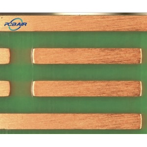
As computational demands for AI models surge, the hardware powering them faces a critical physical limitation: thermal management. Addressing this industry bottleneck, PCBAIR, a specialized PCB manufacturer and assembly provider, today announced significant upgrades to its heavy-copper manufacturing processes. These enhanced capabilities are engineered to manage the extreme power density and heat dissipation requirements of next-generation AI servers and HPC clusters.
With the Thermal Design Power (TDP) of modern AI accelerators and GPUs frequently exceeding 700W per chip, traditional PCB stack-ups are reaching their limits. Standard copper weights are often insufficient for high-current Power Delivery Networks (PDN), leading to excessive I²R losses and thermal buildup.
PCBAIR's upgraded production line now supports precision heavy-copper fabrication of up to 10 oz (approx. 350µm) for both inner and outer layers. This capability allows the PCB to function as a highly efficient heat spreader, significantly reducing reliance on external cooling solutions.
Advanced Fabrication to Overcome Etching Challenges
The upgrade specifically targets common defects in heavy-copper manufacturing, such as "undercutting" (trace narrowing) and "resin starvation" during lamination.
"The PCB has evolved from a passive carrier to an active component of the thermal solution," said Victor Zhang, CTO of PCBAIR. "The real challenge with heavy copper isn't just plating thickness; it is achieving straight sidewalls to ensure electrical performance. Our upgraded process utilizes advanced differential etching compensation and vacuum-assisted resin filling. This ensures we deliver the high-current capacity engineers need, eliminating the micro-voids or delamination risks that often affect thick-copper boards."
Key Technical Enhancements Include:
Embedded Copper Coin Technology: Integration of solid copper "coins" directly into the PCB structure to provide a vertical thermal path from hot components (like Voltage Regulators) to the chassis, overcoming the low thermal conductivity of FR-4 substrates.
Optimized Etching Factor: Proprietary chemical etching protocols that maintain trace width consistency even on 6oz+ layers, crucial for stable impedance in power modules.
High-Reliability Material Qualification: Full compatibility with High-Tg laminates designed to withstand the rigorous thermal cycles of data center environments.
Validated Reliability
To ensure these upgrades meet Tier-1 infrastructure demands, PCBAIR has implemented enhanced reliability testing. Recent internal reports indicate that PCBAIR's heavy-copper prototypes passed 1,000 cycles of thermal shock testing (-40°C to +125°C) with zero continuity failures, validating the robustness of the Plated Through Holes (PTH) and interconnects.
This capability upgrade marks a strategic expansion for PCBAIR, moving beyond standard consumer electronics to support the robust infrastructure required by the global AI and automotive industries. The company is now accepting RFQs for prototyping and low-to-mid volume production of these heavy-copper designs.


