-

-
News
News Highlights
- Books
Featured Books
- smt007 Magazine
Latest Issues
Current Issue
APEX EXPO 2026 Preshow
This month, we take you inside the annual trade show of the Global Electronics Association, to preview the conferences, standards, keynotes, and other special events new to the show this year.

A Look Back at 2025
Innovation rippled across the entire electronics supply chain in 2025, from semiconductor packaging and substrate materials to denser boards and more robust designs. This issue explores these defining moments and what we can expect in the year to come.

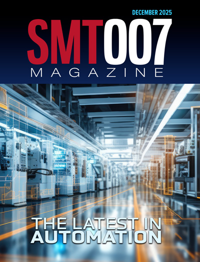
The Latest in Automation
When customer requirements shift, responses range from new equipment to automation. Explore the newest solutions reshaping production and how today’s market dynamics are driving these trends.
- Articles
- Columns
- Links
- Media kit
||| MENU - smt007 Magazine
Estimated reading time: 5 minutes
Powering the Future: From Thick-Film to DBC—Understanding the Evolution of Ceramic Packaging
Ceramic packaging has quietly powered the electronics revolution for more than half a century. From the earliest thick-film hybrids to today’s direct bond copper (DBC) substrates and metallized aluminum nitride, every step forward in ceramic technology has pushed the limits of reliability, power density, and performance. It’s essential for every design engineer building the next generation of electronic systems to understand this evolution.
The Beginning: Thick-Film Technology and the Birth of Reliability
Thick-film was the original workhorse, the first real bridge between circuit design and materials science.
In the 1960s and ’70s, as electronics became smaller and more powerful, traditional printed wiring boards struggled to handle high temperature and voltage environments. Ceramics, particularly aluminum oxide (Al₂O₃), offered a solution: They were strong insulators, dimensionally stable, and capable of surviving where plastics couldn’t.
Thick-film technology emerged to build conductive and resistive layers directly on ceramic substrates. Engineers screen-printed metallic and dielectric pastes—often silver, palladium, or gold—and fired them in furnaces to form durable, adherent traces.
The result was a rugged, compact circuit that could endure thermal cycling and mechanical stress. Thick-film hybrids became the standard for military, aerospace, and medical electronics, providing unmatched reliability in demanding conditions.
Even today, thick-film remains a vital technology. It is flexible, proven, and highly customizable for complex circuit topologies and sensor integration.
The Drive for Power: Enter DBC and Active Metal Brazed (AMB) Substrates
By the 1980s, power electronics were advancing rapidly. Engineers needed substrates that could move large amounts of current and heat, something thick-film struggled to manage.
That led to the next evolutionary leap: direct bond copper (DBC) and active metal brazed (AMB) substrates.
DBC technology bonds a thick copper layer (typically 200–400 µm) directly to a ceramic substrate, usually aluminum oxide or aluminum nitride. The process uses a high-temperature oxidation and bonding reaction to fuse copper and ceramic at the atomic level, with no adhesives or intermediates.
The result was outstanding thermal conductivity and mechanical strength, making DBC ideal for high-power devices like IGBTs, MOSFETs, and SiC modules.
AMB followed soon after, using active-metal brazing alloys (like titanium-based solders) to achieve similar copper-to-ceramic bonds at slightly lower process temperatures, allowing use with beryllia and aluminum nitride for even higher performance.
With DBC and AMB, engineers could finally achieve low thermal resistance and high current capacity in compact, durable packages, perfect for the rising tide of power electronics in industrial drives, automotive inverters, and renewable energy systems.
The Material Revolution: Aluminum Nitride, Silicon Nitride, and Beyond
Ceramic packaging isn’t standing still; it’s evolving at the same pace as semiconductors.
While process innovation was key, material science kept driving the next wave of change. Aluminum nitride (AlN) entered mainstream production in the 1990s, offering thermal conductivity up to 180 W/m·K, nearly eight times higher than alumina, and with excellent dielectric strength.
Then came silicon nitride (Si₃N₄), a material with slightly lower conductivity but dramatically better mechanical toughness and thermal shock resistance. Silicon nitride’s ability to survive vibration and cycling made it ideal for EV traction inverters, aerospace converters, and rail power modules, where reliability literally determines safety.
These new materials allowed engineers to push junction temperatures higher, reduce cooling requirements, and increase power density, thus fundamentally changing what was possible in electronic packaging.
Why the Evolution Matters: Design Realities in Today’s Systems
The shift from thick-film to DBC isn’t about replacing old technology, but rather about matching the right tool to the job.
Thick-film remains unmatched for mixed-signal circuits, hybrid modules, and sensor assemblies that require fine geometry and multilayer capability. It’s cost-effective, flexible, and ideal for moderate-power applications.
DBC and AMB, on the other hand, dominate where heat flux, current load, and structural reliability are mission-critical.
Design engineers must now balance multiple variables:
- Thermal conductivity vs. mechanical strength (AlN vs. Si₃N₄)
- Cost vs. performance (alumina vs. AlN)
- Metallization type vs. process compatibility (thick-film vs. direct copper bonding)
- CTE matching between substrate, copper, and attached devices
This goes beyond materials science to system engineering. A substrate that saves 5°C in junction temperature can extend device life by years and allow downsizing of the heat sink, saving weight and cost across the system.
Integration and Miniaturization: The Hybrid Future
We’re entering an era where the line between ‘substrate’ and ‘circuit’ is disappearing.
As design density climbs, engineers are merging the advantages of multiple technologies. Today, we see hybrid DBC-thick-film modules where fine-line screen printing adds passive components, resistors, or signal routing directly atop DBC copper.
We’re also seeing multi-layer ceramic architectures, embedded metal vias, and direct chip attach techniques that turn the substrate into an active participant in circuit performance.
At Remtec, we often help customers combine thick-film precision with DBC strength, especially in RF power amplifiers, LED drivers, and high-current converters. The result is a substrate that’s both intelligent and indestructible, capable of carrying data and dissipating heat with equal reliability.
Design Considerations for Modern Engineers
Understanding the evolution of ceramic packaging helps engineers make smarter design choices today. When selecting substrate technology, consider:
- Power and heat load: DBC and AMB offer the lowest thermal resistance for high-power applications.
- Electrical Performance: Thick-film provides excellent signal integrity and customization for complex circuits.
- Mechanical Stress and Environment: Silicon nitride substrates excel in shock, vibration, and high-temperature cycling.
- Manufacturing Compatibility: Choose metallization systems that align with your assembly methods: solder attach, wire bond, epoxy, or sintering.
- Lifecycle Cost: The most expensive substrate may be the cheapest over time if it eliminates field failures.
- Design is about trade-offs and the best engineers are those who understand the invisible physics behind those decisions.
The Next Frontier: Additive and Advanced Metallization
The future of ceramic packaging is additive. We’re now developing laser-patterned, inkjet-printed, and 3D additive metallization processes that combine the precision of thick-film with the efficiency of DBC.
These technologies will enable faster prototyping, localized reinforcement of heat paths, and even embedded temperature-sensing structures within substrates. Imagine a DBC board that monitors its own health in real time; that’s where we’re headed.
At Remtec, we’re investing heavily in metallization science and surface engineering, because the interface—where metal meets ceramic—is where performance is either made or lost.
Ceramic Packaging
Ceramic packaging may not grab headlines like AI or quantum computing, but it’s the quiet backbone that keeps modern electronics alive. From the thick-film circuits that powered early satellites to the DBC substrates driving today’s electric vehicles, every innovation builds on a foundation of reliable materials and precise manufacturing.
The best engineers never stop learning how those materials evolve, because every advancement in ceramics is an opportunity to build something smaller, faster, cooler, and tougher than before.
Powering the future starts with understanding the past, one layer, one bond, and one breakthrough at a time.
This column originally appeared in the February 2026 issue of SMT007 Magazine.


