














 Knocking Down the Bone Pile: Hot Air vs. Infrared PCB Rework
 Nolan’s Notes: Why Mexico’s Time Has Come
 Standard of Excellence: ‘Quality’ Is Your Company's Greatest Competitive Advantage






As silicon scaling becomes more expensive, advanced packaging is becoming a key enabler for system-level integration and performance enhancement.
Over the past several years, advanced packaging has moved from the back end of semiconductor manufacturing to becoming one of the electronics industry's most strategic technologies in the ecosystem. At many IEEE conferences, discussions that once centered almost exclusively on transistor scaling now devote equal attention to chiplets, heterogeneous integration, co-design, advanced substrates, thermal management, and system-level packaging.
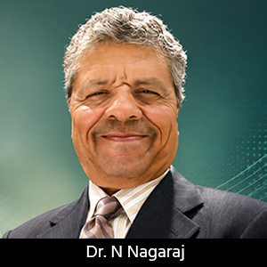
That broader shift formed the backdrop of a recent webinar presented by Dr. Devan Iyer, chief strategist for advanced electronic packaging at the Global Electronics Association, for SemiX Bombay and the IEEE Power Electronics Society & IEEE Industrial Electronics Society. Dr. Iyer draws on more than four decades of experience spanning semiconductor design, assembly, manufacturing, and advanced packaging to explain why packaging, thermal management, and system-level co-design are now inseparable.
"The future of semiconductor based systems," Iyer said during his presentation, "will increasingly be enabled by innovations in packaging rather than device scaling alone."
That conclusion reflects a growing consensus throughout the semiconductor ecosystem. Whether discussing chiplet architectures, AI hardware platforms, wireless connectivity solutions, or EV electronics, packaging has become a competitive differentiator rather than simply a manufacturing step. System performance depends on how efficiently and cost-effectively designers integrate heterogeneous technologies into a single package while managing signal integrity, power delivery, thermal management, and form factor to meet the required reliability.
Power Electronics
"Power requirements are everywhere," said Iyer, pointing to EVs, renewable energy systems, industrial automation, robotics, aerospace, AI infrastructure, and HPC, all of which depend on efficient power conversion. These applications share remarkably similar engineering requirements: managing higher voltages, greater current densities, faster switching speeds, and significantly more heat than previous generations of electronics.
Wide-bandgap semiconductors such as silicon carbide (SiC) and gallium nitride (GaN) promise dramatic improvements in efficiency and power density. But realizing those gains now depends as much on packaging as it does on the semiconductor devices themselves. Package/module design from electrical, thermal, and mechanical perspectives; materials selection; interconnect assembly and substrate technology; thermal interfaces and cooling solutions; and testing all influence overall performance and reliability.
AI Infrastructure Learning from Power Electronics
One of the most intriguing observations during the webinar is the convergence occurring between AI infrastructure and power electronics. The thermal challenges facing today's AI accelerators resemble those long encountered by power electronics engineers. At first glance, GPUs powering AI clusters and high-voltage industrial power modules seem to have little in common; one processes information, while the other deals with power conversion. Yet both are rapidly encountering the same limitations.
GPUs that approach, and in some cases exceed, one kilowatt of dissipation are forcing data center designers to adopt liquid cooling, advanced thermal interface materials, vapor chambers, and sophisticated package architectures once associated primarily with industrial power systems. The same is true for AI accelerators.
According to Dr. Iyer, the power electronics community has been developing these solutions for many years. That convergence reflects a broader reality: advanced computing and advanced power systems are becoming increasingly intertwined. The engineering disciplines, and the people developing them, are beginning to overlap.
For the packaging community, that creates opportunities for technologies originally developed for one market to migrate rapidly into another. "The data center packaging engineers and power electronics packaging engineers are sitting in the same room in the companies today," Iyer said.
Co-Design: The New Engineering Model
As packaging becomes more important, the way products are developed is also changing. Co-design has likewise become a defining theme in the semiconductor supply chain. Rather than optimizing devices, packages, substrates, and manufacturing independently, companies increasingly assemble multidisciplinary development teams from the earliest design stages. Device physicists, package designers, PCB engineers, and reliability experts begin to work concurrently, recognizing that decisions made in one discipline inevitably affect performance in another.
Historically, semiconductor devices, packages, materials, manufacturing, and reliability were optimized independently before being integrated into a finished product. That approach is becoming impractical. "Chip-package co-design is extremely important," Iyer said.
Whereas electrical performance affects thermal behavior, material selection influences electrical performance, and manufacturing processes impact reliability. Mechanical stresses influence long-term performance. So, every engineering decision now affects several others. The result is a growing emphasis on co-design that brings device engineers, package designers, materials scientists, manufacturing specialists, reliability engineers, and thermal experts together much earlier in product development.
DFM, design for reliability (DFR), and design for test (DFT) are no longer sequential activities. They have become interconnected elements of a single engineering process.
This philosophy also extends into manufacturing itself. Technologies such as silver sintering, copper clip bonding, embedded power modules, advanced ceramic substrates, AI-assisted defect detection, predictive reliability modeling, and digital twins all reflect an industry moving toward optimization of the complete system rather than individual components.
Packaging's Expanding Role
Looking ahead, Iyer said, advanced packaging is the bridge connecting semiconductor devices, substrates, PCBs, cooling systems, materials, manufacturing processes, and ultimately complete electronic systems—an evolution transforming packaging from a supporting function into one of strategic importance in the electronics ecosystem.
For packaging professionals like Iyer, that evolution represents both a challenge and an opportunity. Advanced electronic packaging is now a primary technology for determining how much performance modern electronic systems can ultimately deliver, and as AI infrastructure expands, electrification accelerates, and heterogeneous integration becomes the industry norm, packaging will steadily move from the background to center stage.
For the engineers working in this field, that may be the most significant development of all.


