-

- News
- Books
Featured Books
- smt007 Magazine
Latest Issues
Current Issue
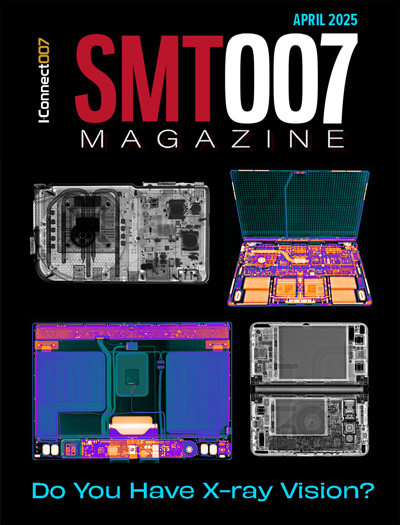
Do You Have X-ray Vision?
Has X-ray’s time finally come in electronics manufacturing? Join us in this issue of SMT007 Magazine, where we answer this question and others to bring more efficiency to your bottom line.

IPC APEX EXPO 2025: A Preview
It’s that time again. If you’re going to Anaheim for IPC APEX EXPO 2025, we’ll see you there. In the meantime, consider this issue of SMT007 Magazine to be your golden ticket to planning the show.

Technical Resources
Key industry organizations–all with knowledge sharing as a part of their mission–share their technical repositories in this issue of SMT007 Magazine. Where can you find information critical to your work? Odds are, right here.
- Articles
- Columns
Search Console
- Links
- Media kit
||| MENU - smt007 Magazine
Shock Reliability of BGAs Using Underfill
December 31, 1969 |Estimated reading time: 5 minutes
SAC BGA packages are known to be more brittle than tin/lead BGAs at high stress levels such as drop testing. This article details a study exploring differences in the reliability of capillary and no-flow underfill for tin/lead and lead-free applications.
By Jim Hisert, Indium Corporation
It is commonly known that Sn/Ag/Cu (SAC) BGA packages are more brittle than tin/lead BGAs at high stress levels, such as those induced during drop testing.1 This problem is remedied by reinforcing solder joints with underfill. Even tin/lead area-array packages are not always sufficiently secure if attached without underfill.
Underfills have been designed to fortify both tin/lead and lead-free packages. Currently, the electronics industry can choose from a few different underfill processes - two of the most popular are capillary underfill (CUF) and no-flow underfill (NFUF). In a drop-test designed to mimic the realistic abuse of portable electronics, packages assembled using each process were tested.
Underfill Overview
Capillary and no-flow underfills are used to improve the drop-test reliability of BGA packages during 2nd level assembly. Capillary underfill is used in the electronics industry to encapsulate the interconnections of flip-chip and BGA packages (Figure 1). No-flow is an underfill technology that has been revisited recently as new materials have made this process more viable (Figure 2).
 Figure 1. No-flow underfill process.
This article focuses on an underfill study performed to examine differences in the reliability of capillary and no-flow underfill for tin/lead and lead-free applications. A similar capillary underfill was used for both tin/lead and lead-free applications, while specific no-flow underfills were used for the two alloy variations. Because capillary underfills require a secondary curing process, these remain the same for different alloys. However, because no-flow underfills act as a flux and cure during initial assembly reflow, they are created differently to accommodate either tin/lead or lead-free reflow temperatures. All tests were performed using daisy-chained PBGA 196 dummy components. This package size was selected to simulate common packages used in portable electronic devices.
No-flow Processing
Assembly of NFUF components. For this analysis, underfill was dispensed manually onto each OSP pad area in a “cross-and-dot” pattern. OSP was chosen as the surface finish for this test because its solderability is more challenging compared to other common finishes (Figure 3). The “cross-and-dot” pattern was implemented to ensure underfill flowed to the corners of the component and pad area.
 Figure 2. Capillary underfill process.
Approximately 100 mg of tin/lead underfill was dispensed onto the pad area, and a tin/lead BGA was placed onto the deposit. The pick-and-place machine was adjusted to 12 psi of placement force, which was enough to spread the underfill from the dispense pattern to the entire area under the BGA. Three BGAs were placed onto each test board, and the boards were ready for reflow because the underfill also contained a flux. The boards were reflowed in a standard tin/lead profile. All steps were repeated with SAC 405 BGAs using the lead-free underfill and a standard linear ramp-to-peak lead-free profile.
Capillary Processing
Assembly of CUF Packages. The capillary underfill process requires considerably more time than the no-flow process. It should also be noted that a low-residue flux was used in the underfill preparation. This was important to create the maximum adherence of the capillary underfill to the BGA’s laminate substrate. First, a flux reservoir was prepared, and leveled to 0.004" (0.1 mm). Next, a tin/lead BGA was dipped in the flux pool to obtain the proper amount of flux on each bump. After the tin/lead BGAs were placed, they were reflowed using the tin/lead profile.
 Figure 3. Wetting/spread of SAC 387 with no-flow underfill in various substrates.
Once the assemblies cooled, they were underfilled with a capillary underfill at an elevated temperature of 80°C to ensure proper flow of the material from the sides of the package to the area underneath the package. The underfill was cured during an additional process at 150°C for 15 minutes.
Test Results
After the samples were assembled, they were attached to a weighted assembly and drop-tested. This drop-test was designed to simulate real-world abuse of portable electronics. Initially, a baseline was developed by testing² components that were not underfilled. They survived only 4-8 drops before losing electrical continuity.
 Figure 4. Edge-drop test assembly.
The underfilled samples were weighted with 32 grams to mimic the mass of a small portable device (Figure 4). Each sample was dropped from six feet (1.8 meters) onto a concrete floor. All samples - tin/lead and lead-free - capillary or no-flow underfilled, survived 3,000 drop cycles. After 3,000 drops onto a concrete floor, other electronic components, and the circuit board itself, have no chance of functioning at all.
This test did not prove which underfill technology is more reliable, but instead proved that, if processed properly, both capillary and no-flow underfill can improve shock resistance (Figure 5). In most cases, it makes sense to choose an underfill that complements the assembly process.3
Conclusion
The material properties of today’s common lead-free solders present a challenge to finished-goods reliability. Underfills enhance the robustness of lead-free solder interconnections - beyond that of traditional non-underfilled tin/lead.
 Figure 5. Edge-drop test results.
Capillary and no-flow underfills each offer unique advantages. Capillary underfills provide a solution for packages that must be reinforced post-facto. No-flow underfills can offer great drop-in replacements for high-density interconnect (HDI) flux or paste. Both solutions improve the reliability of a user’s finished goods by over two orders of magnitude, while adding only a marginal amount of production costs. Increased reliability can easily translate into profitability for the user through the reduction of field failures and improved product image in the market.
REFERENCES
- Ning-Cheng Lee, “The Relationship of Components, Alloys and Fluxes,” PCD&M, October/November 2005.
- Dr. Wusheng Yin and Dr. Ning-Cheng Lee, “Reworkable No-flow Underfilling For Both Tin-lead and Lead-free Reflow Assembled Under Air,” SMTAI, 2005.
- Wusheng Yin, Geoffrey Beckwith, Hong-Sik Hwang, and Ning-Cheng Lee, “Low Cost No-flow Underfill Being a Reality for Manufacturing,” NEPCON West, 2002.
Jim Hisert, applications engineer for semiconductor materials, Indium Corporation, may be contacted at (315) 853-4900; e-mail: jhisert@indium.com.


