


 Global Citizenship: Together for a Perfect PCB Solution
 Smart Automation: Odd-form Assembly—Dedicated Insertion Equipment Matters
 Nolan’s Notes: Everyone Has Their Eye on India


Miniaturization with the Help of Reduced Component-to-Component Spacing
May 27, 2015 | J. Sjoberg, R. Aranda, D. Geiger, A. Mohammed and M. Kurwa, Flextronics AEGEstimated reading time: 2 minutes
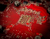
With the never-ending drive for smaller, lighter and more advanced features on portable products, the ability to handle miniaturization is becoming a key capability to enable these requirements. Miniaturization can be done in many ways and this article touches on the assembly technologies that can be incorporated in a more or less standard surface mount assembly line with minimal equipment and material upgrades.
Before starting any development work it is critical to understand product and industry requirements and capabilities. If this is not fully understood, no development activities can start. PCB fabrication can be seen as a good example on the importance of understanding requirements and capabilities. If a good quality PCB can’t be sourced within the scope of the assembly development project there is no reason to develop an assembly technology process since there is not anything to do the assembly development work on. The key is to ensure that several options for assembly can be achieved and this should be seen as a toolbox of technologies.
For the active components die stacking inside a package is one common way to increase the functionality per unit area on a PCBA, which is very popular for memory devices. However, there can be some drawbacks to creating a stacked die solution. First, this method is a customized solution. If any of the dies to be used changes, the die stack needs to be evaluated to see if changes are needed in the package. For example, a die shrink may occur and this could change the whole package structure. Secondly, if one or more of the dies inside the package fail, the whole unit will have to be scrapped, which would lead to increased cost; this is the well-known compounded yield issue. Lastly, trying to coordinate the many semiconductor suppliers to provide dies to a packaging house for die stacking can be a challenging task and overall responsibility for the complete package yield could in some cases be unclear.
In the PoP process one component is placed on top of another package during a single SMT process to fully utilize the three dimensional aspect of the product. The topside of the bottom component has pads similar to the pads on the PCB for attachment of the top package. Each package is a single unit that can be fully tested as a normal IC package is done today, so the yield would be comparable to the normal yield commonly seen today. Another advantage would be the ability to have second-source options that could be fairly easily inserted into the process.
The stacked package can be processed in a traditional SMT environment with a few upgrades that are readily available. Therefore, package stacking enables configurable assemblies and provides greater flexibility in the supply chain. It can be used for memory applications or for a processor with memory, with faster time to market and better management of package testing and compounded yield issues.
Editor's Note: This article originally appeared in the May 2015 issue of SMT Magazine.
Share on:


Testimonial
"The I-Connect007 team is outstanding—kind, responsive, and a true marketing partner. Their design team created fresh, eye-catching ads, and their editorial support polished our content to let our brand shine. Thank you all! "
Sweeney Ng - CEE PCBSuggested Items
Variosystems Strengthens North American Presence with Southlake Relaunch 2025
09/15/2025 | VariosystemsVariosystems celebrated the relaunch of its U.S. facility in Southlake, Texas. After months of redesign and reorganization, the opening marked more than just the return to a modernized production site—it was a moment to reconnect with our teams, partners, and the local community.
MacDermid Alpha Presents at SMTA New Delhi, Bangalore Chapter, on Flux–OSP Interaction
09/09/2025 | MacDermid Alpha Electronics SolutionsMacDermid Alpha contributes technical insights on OSP solderability at the Bangalore Chapter, SMTA reinforcing commitment to knowledge-sharing and industry collaboration.
Naprotek Appoints Mark Crebs to Lead Business Development for Products and Platforms
08/27/2025 | Naprotek LLCNaprotek, LLC, a leading provider of mission-critical electronics technology solutions, announced the appointment of Mark Crebs to Products and Platform Director of Business Development.
VVDN Expands Manufacturing Footprint into the UAE to Meet Global Demand
08/20/2025 | PRNewswireVVDN Technologies, a global provider of software, product engineering and electronics manufacturing services & solutions, today announced it is setting up a new manufacturing facility in the UAE as part of its global expansion strategy.
SisTech Manufacturing Expands Services: Leading Precision in Electronic Manufacturing
08/11/2025 | Globe NewswireSisTech Manufacturing, known for its expertise in precision electronic manufacturing services, is expanding what it can do in production. For over 30 years, the company has been recognized for its commitment to quality and its ability to meet the diverse demands of industries like aerospace and consumer electronics. With ISO 9001:2015 certification and ITAR registration,