-
-
News
News Highlights
- Books
Featured Books
- smt007 Magazine
Latest Issues
Current IssueMoving Forward With Confidence
In this issue, we focus on sales and quoting, workforce training, new IPC leadership in the U.S. and Canada, the effects of tariffs, CFX standards, and much more—all designed to provide perspective as you move through the cloud bank of today's shifting economic market.
Intelligent Test and Inspection
Are you ready to explore the cutting-edge advancements shaping the electronics manufacturing industry? The May 2025 issue of SMT007 Magazine is packed with insights, innovations, and expert perspectives that you won’t want to miss.
Do You Have X-ray Vision?
Has X-ray’s time finally come in electronics manufacturing? Join us in this issue of SMT007 Magazine, where we answer this question and others to bring more efficiency to your bottom line.
- Articles
- Columns
- Links
- Media kit
||| MENU - smt007 Magazine
A Rework Dilemma: PCB Shields
July 15, 2015 | Bob Wettermann, BEST Inc.Estimated reading time: 1 minute

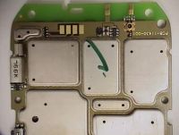
RF shields minimize radio frequency (RF) noise to prevent it from affecting the sensitive and critical electronic components beneath the shield. They also prevent such noise from interfering with neighboring devices or other systems in the vicinity. RF shields typically have a unique design and conform to the layout of the PCB. Often, the shields are not regular-shaped designs; rather, they are designed and are shaped by the PCB layout. Typically, these shields can be found on handheld wireless device PCBs such as smartphones, netbooks, tablets, portable medical devices and audio/video players, to name a few.
There are two basic construction types for these shields. Some of them are a two-piece construction with a "fence" soldered to the PCB and a cover fitted over this fence.
Other shields are a one-piece construction with an open-sided can overlaying the components and soldered to the PCB. These one-piece shields are a serious challenge to rework and will be the focus of this rework discussion.
Challenges of shield rework
There are numerous challenges associated with reworking shields, including, but not limited to:
1. Devices are very tight and close to the shield itself—many times within a few millimeters. This means that the rework process, if not precisely controlled, can present problems in disturbing nearby devices.
2. Shield trace solder excavation and PCB board prep are challenging as well, especially for odd-shaped shields. Manual methods require extreme dexterity as the distance between the land of the shield and neighboring devices is very small. This means that neighboring devices can be disturbed.
Resoldering of the shields can be very challenging as the gap between the shield lip and the board needs to be closed so as to not allow for any ingress or egress (in some cases) of RF signals. This means there is little room for error.
Editor's Note: This article originally appeared in the July 2015 issue of SMT Magazine.
Suggested Items
Indium Corporation Expert to Present on Automotive and Industrial Solder Bonding Solutions at Global Electronics Association Workshop
06/26/2025 | IndiumIndium Corporation Principal Engineer, Advanced Materials, Andy Mackie, Ph.D., MSc, will deliver a technical presentation on innovative solder bonding solutions for automotive and industrial applications at the Global Electronics A
Fresh PCB Concepts: Assembly Challenges with Micro Components and Standard Solder Mask Practices
06/26/2025 | Team NCAB -- Column: Fresh PCB ConceptsMicro components have redefined what is possible in PCB design. With package sizes like 01005 and 0201 becoming more common in high-density layouts, designers are now expected to pack more performance into smaller spaces than ever before. While these advancements support miniaturization and functionality, they introduce new assembly challenges, particularly with traditional solder mask and legend application processes.
Knocking Down the Bone Pile: Tin Whisker Mitigation in Aerospace Applications, Part 3
06/25/2025 | Nash Bell -- Column: Knocking Down the Bone PileTin whiskers are slender, hair-like metallic growths that can develop on the surface of tin-plated electronic components. Typically measuring a few micrometers in diameter and growing several millimeters in length, they form through an electrochemical process influenced by environmental factors such as temperature variations, mechanical or compressive stress, and the aging of solder alloys.
SolderKing’s Successful Approach to Modern Soldering Needs
06/18/2025 | Nolan Johnson, I-Connect007Chris Ward, co-founder of the family-owned SolderKing, discusses his company's rapid growth and recent recognition with the King’s Award for Enterprise. Chris shares how SolderKing has achieved these award-winning levels of service in such a short timeframe. Their secret? Being flexible in a changing market, technical prowess, and strong customer support.
Preventing Surface Prep Defects and Ensuring Reliability
06/10/2025 | Marcy LaRont, PCB007 MagazineIn printed circuit board (PCB) fabrication, surface preparation is a critical process that ensures strong adhesion, reliable plating, and long-term product performance. Without proper surface treatment, manufacturers may encounter defects such as delamination, poor solder mask adhesion, and plating failures. This article examines key surface preparation techniques, common defects resulting from improper processes, and real-world case studies that illustrate best practices.