


 Dan’s Biz Bookshelf: Four Important Books You Need to Read (Not Just Say You Have)
 The Marketing Minute: Cracking the Code of Technical Marketing


Shortest Wavelength Plasmons in Single Walled Nanotubes
July 29, 2015 | Lawrence Berkeley National LaboratoryEstimated reading time: 3 minutes
The term “plasmons” might sound like something from the soon-to-be-released new Star Wars movie, but the effects of plasmons have been known about for centuries. Plasmons are collective oscillations of conduction electrons (those loosely attached to molecules and atoms) that roll across the surfaces of metals while interacting with photons. For example, plasmons from nanoparticles of gold, silver and other metals interact with visible light photons to generate the vibrant colors displayed by stained glass, a technology that dates back more than 1,000 years. But plasmons have high-technology applications as well. In fact, there’s even an emerging technology named for them – plasmonics – that holds great promise for superfast computers and optical microscopy.
At the heart of the high-technology applications of plasmons is their unique ability to confine the energy of a photon into a spatial dimension smaller than the photon’s wavelength. Now, a team of researchers with Berkeley Lab’s Materials Sciences Division, working at the Advanced Light Source (ALS), has generated and detected plasmons that boast one of the strongest confinement factors ever: the plasmon wavelength is only one hundredth of the free-space photon wavelength.
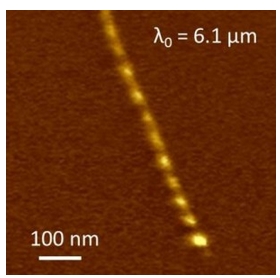
By focusing infrared light onto the tip of an Atomic Force Microscope, the researchers were able to observe what are called “Luttinger-liquid” plasmons in metallic single-walled nanotubes. A Luttinger-liquid is the theory that describes the flow of electrons through one-dimensional objects, such as a single-walled nanotube (SWNT), much as the Fermi-liquid theory describes the flow of electrons through most two- and three-dimensional metals.
“It is amazing that a plasmon in an individual nanotube, a 1-D object barely a single nanometer in diameter, can even be observed at all,” says Feng Wang, a condensed matter physicist with Berkeley Lab’s Materials Sciences Division who led this work. “Our use of scattering-type scanning near-field optical microscopy (s-SNOM) is enabling us to study Luttinger-liquid physics and explore novel plasmonic devices with extraordinary sub-wavelength confinement, almost 100 million times smaller in volume than that of free-space photons. What we’re observing could hold great promise for novel plasmonic and nanophotonic devices over a broad frequency range, including telecom wavelengths.”
Wang, who also holds appointments with the University California (UC) Berkeley Physics Department and the Kavli Energy NanoScience Institute (Kavli-ENSI), is the corresponding author of a paper in Nature Photonics that describes this research. The paper is titled “Observation of a Luttinger-liquid plasmon in metallic single-walled carbon nanotubes.” The co-lead authors are Zhiwen Shi and Xiaoping Hong, both members of Wang’s UC Berkeley research group. Other co-authors are Hans Bechtel, Bo Zeng, Michael Martin, Kenji Watanabe, Takashi Taniguchi and Yuen-Ron Shen.
Despite the enormous potential of plasmons for the integration of nanoscale photonics and electronics, the development of nanophotonic circuits based on classical plasmons has been significantly hampered by the difficulty in achieving broadband plasmonic waveguides that simultaneously exhibit strong spatial confinement, a high quality factor and low dispersion. The observations of Wang and his colleagues demonstrate that Luttinger-liquid plasmon of 1-D conduction electrons in SWNTs behaves much differently from classical plasmons.
“Luttinger-liquid plasmons in SWNTs propagate at semi-quantized velocities that are independent of carrier concentration or excitation wavelength, and simultaneously exhibit extraordinary spatial confinement, a high quality factor and low dispersion,” says co-lead author Shi. “Usually, to be manipulated efficiently with a photonic device, the light wavelength is required to be smaller than the device. By concentrating photon energy at deep sub-wavelength scales, Luttinger-liquid plasmons in SWNTs effectively reduce the light wavelength. This should allow for the miniaturization of photonic devices down to the nanometer scale.”
Wang, Shi, Hong and their colleagues observed Luttinger-liquid plasmons using the s-SNOM setup at ALS Beamline 5.4.1. Metallic SWNTs with diameters ranging from 1.2 to 1.7 nanometers were grown, purified and then deposited on a boron nitride substrate. Single wavelength infrared light was focused onto the tip of an Atomic Force Microscope to excite and detect a plasmon wave along an SWNT.
“Our direct observation of Luttinger-liquid plasmons opens up exciting new opportunities,” Wang says. “For example, we’re now exploring these plasmons in telecom wavelengths, the most widely used in photonics and integrated optics. We’re also learning how the properties of these plasmons might be manipulated through electrostatic gating, mechanical strain and external magnetic fields.”
This research was primarily supported by the U.S. Department of Energy’s Office of Science.
Share on:


Testimonial
"Our marketing partnership with I-Connect007 is already delivering. Just a day after our press release went live, we received a direct inquiry about our updated products!"
Rachael Temple - AlltematedSuggested Items
The Shaughnessy Report: Winning the Signal Integrity Battle
09/09/2025 | Andy Shaughnessy -- Column: The Shaughnessy ReportWhen I first started covering this industry in 1999, signal integrity was the hip new thing in PCB design. Conference classes on signal integrity were packed to the walls, and an SI article was guaranteed to get a lot of reads.
Standard of Friendship: Debbie McDade and Symon Franklin Went From Classmates to Colleagues
08/27/2025 | Debbie McDade, Advanced Rework Technology Ltd.As a fairly new IPC Master Trainer, I nervously attended my first IPC committee meeting in 2002 in New Orleans—a 4,600-mile trip from my home in the UK—for the IPC-610 Task Group. With more than 250 members, it was the largest IPC committee at that time.
New Frontier Aerospace and Air Force Institute of Technology Sign CRADA to Advance Hypersonic VTOL Aircraft
08/05/2025 | PR NewswireNew Frontier Aerospace (NFA) is excited to announce a Collaborative Research and Development Agreement (CRADA) with the Air Force Institute of Technology (AFIT) aimed at advancing an innovative rocket-powered hypersonic Vertical Takeoff and Landing (VTOL) aircraft.
Insulectro Facilitates Fabricator Access to EMC Mass Lam Capabilities
07/30/2025 | InsulectroInsulectro, the largest distributor of materials used in the manufacturing of printed circuit boards and printed electronics, announces a new service - a system to help our customers to access EMC's well established mass lam offerings. Long a leader in mass lam manufacturing, EMC is the exclusive supplier in Insulectro's laminate and pre preg portfolio.
American Made Advocacy: A Growing Presence in Washington in Turbulent Times
07/29/2025 | Shane Whiteside -- Column: American Made AdvocacyLast month, PCBAA held its fourth annual meeting in Washington, D.C. It was our largest gathering to date and included speakers from the House and Senate, the Department of Commerce, and OEMs Lockheed Martin, RTX, and Northrop Grumman. We also spent a day on Capitol Hill educating lawmakers and their staff about the importance of a secure domestic microelectronics supply chain.