-

- News
- Books
Featured Books
- smt007 Magazine
Latest Issues
Current Issue
The Path Ahead
What are you paying the most attention to as we enter 2025? Find out what we learned when we asked that question. Join us as we explore five main themes in the new year.

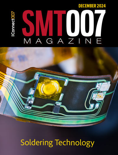
Soldering Technologies
Soldering is the heartbeat of assembly, and new developments are taking place to match the rest of the innovation in electronics. There are tried-and-true technologies for soldering. But new challenges in packaging, materials, and sustainability may be putting this key step in flux.

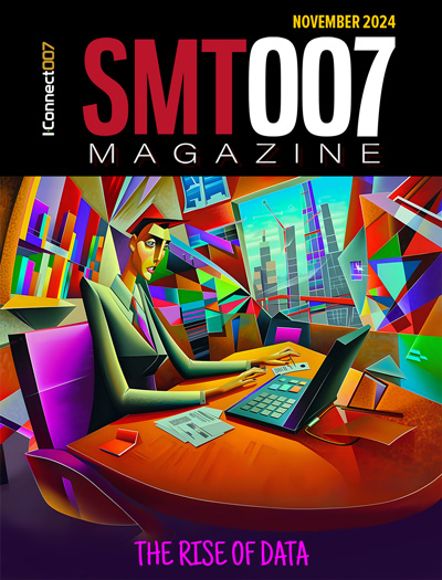
The Rise of Data
Analytics is a given in this industry, but the threshold is changing. If you think you're too small to invest in analytics, you may need to reconsider. So how do you do analytics better? What are the new tools, and how do you get started?
- Articles
- Columns
Search Console
- Links
- Media kit
||| MENU - smt007 Magazine
Exploring Nanoscale Structure of Thin Films
August 4, 2015 | Brookhaven National LaboratoryEstimated reading time: 5 minutes
The world’s newest and brightest synchrotron light source—the National Synchrotron Light Source II (NSLS-II) at the U.S. Department of Energy’s Brookhaven National Laboratory—has produced one of the first publications resulting from work done during the facility's science commissioning phase.
Published July 7 in the online edition of the International Union of Crystallography Journal (a recently launched journal of the International Union of Crystallography), the paper discusses a new way to apply a widely used local-structure analysis tool—known as atomic pair distribution function (PDF) analysis—to x-ray scattering data from thin films, quickly yielding high-quality information on the films' atomic structure. The work creates new avenues for studies of nanocrystalline thin films.
This work shows that NSLS-II—a DOE Office of Science User Facility with ultra-bright, ultra-concentrated x-ray beams—is already proving to be a game-changer in studies of thin films, which play a vital role in a large number of technologies, including computer chips and solar cells.
Simon Billinge, author on the paper and a physicist with a joint position at Brookhaven National Laboratory and Columbia University's School of Engineering and Applied Science.
Thin film challenges
In applications and during experiments, thin films (defined as having thicknesses from just a few to more than 1000 nanometers, or billionths of a meter) are deposited onto a thick base, called a substrate, often made of crystalline wafers of silicon, silicon dioxide, or aluminum oxide. It is extremely difficult to study the structure of materials in this geometry because of the small amount of film material and large amount of substrate. To minimize the scattering of x-rays off the substrate, which tends to obscure the data from the tiny volume of sample, thin film x-ray studies are done using grazing incidence (GI) x-ray experiments.
In GI studies, the x-ray beam grazes the surface of the film such that it reflects off the substrate, allowing the beam to illuminate as much of the film as possible while minimizing penetration through the film into the substrate. However, the small angle of incidence makes GI studies notoriously difficult to carry out and introduces serious complexities in data analysis.
“Grazing-incidence diffraction experiments are tricky for crystalline materials, and have never successfully been done to obtain PDFs from films,” said one of the paper's authors, Simon Billinge, a physicist with a joint position at Brookhaven and Columbia University's School of Engineering and Applied Science. “The experiments are too painstaking and the data analysis is extremely challenging.”
Studying the ‘atomic neighborhood’
PDF provides local atomic structural information – that is, data for neighborhoods of atoms – by yielding the distances between all pairs of atoms in the sample. These distances appear as peaks in the data. In recent years, PDF has become a standard technique in structural studies of complex materials and can be used for samples that are bulk or nanoscale, amorphous or crystalline.
The approach that Billinge and his colleagues devised leverages the high fluxes of photons coming from NSLS-II, which, together with novel data reduction methods recently developed in his group, creates data suitable for PDF analysis from a thin film. Essentially, it turns the standard GI experiment on its head: the beam is simply sent through the film from the back to the front.
Eric Dooryhee, the lead scientist for the NSLS-II X-Ray Powder Diffraction (XPD) beamline, where the work was done, explained, “The first group of NSLS-II beamlines is now successfully transitioning from technical commissioning, which began back in the fall of 2014 when we first produced x-ray light, towards science commissioning, where we benchmark and test the beamline capabilities on real samples. Extracting the thin film's tiny signal from the substrate's large signal in this normal-incidence geometry is extremely technically difficult. Nonetheless, I told Simon that XPD should be up to the challenge.”
Preview of future breakthroughs
This is an exciting new result by itself, but it only gives us a glimpse of the possibilities that NSLS-II will present as the power ramps up over the next few years. This is the tip of the iceberg of what will be possible when NSLS-II is operating at full power.
— Simon Billinge
The group tested thin-film PDF (which they call tfPDF) with both crystalline and amorphous thin films, each about 360 nm thick. The collaboration includes the groups of Bo Iversen at Aarhus University in Denmark and Dave Johnson from the University of Oregon, who prepared the thin films.
The first sample studied was an amorphous iron-antimony film on an amorphous borosilicate substrate mounted perpendicular to the x-ray beam. In order to isolate the contribution from the film, the substrate contribution was first determined by measuring the scattering pattern from a clean substrate. The signal from the film is barely visible in the raw data on top of the large substrate contribution, but could be clearly extracted during data processing. This allowed for a reliable, low-noise PDF that can be modeled successfully to yield the quantitative atomic structure of the film.
The data led to high-quality PDFs for both amorphous and crystalline films—confirmed by comparison to control samples in a standard PDF setup. Based on the success of these first measurements, the Billinge group and the XPD team are now planning future experiments to watch the films crystallize in real time, in the beam.
“The discovery that we can get PDFs from samples in thin-film geometry so readily will revolutionize this area of science,” said Kirsten Jensen, a postdoctoral researcher in Billinge’s group at Columbia. “The experiments don’t take any specialized equipment or expertise beyond the beamline setup at XPD and are quick, opening the way to time-resolved in-situ studies of changes in film structure under processing as well as spatially resolved studies of nanostructured films in place.”
Added Billinge, “This is an exciting new result by itself, but it only gives us a glimpse of the possibilities that NSLS-II will present as the power ramps up over the next few years. This is the tip of the iceberg of what will be possible when NSLS-II is operating at full power.”
NSLS-II is supported by the U.S. Department of Energy's Office of Science. Support for this study was also provided by the Villum Foundation Postdoc Program, the Sino-Danish Center, the National Science Foundation, and the Danish National Research Foundation.
Suggested Items
BAE Systems Awarded $85M Contract to Deliver Network Tactical Common Data Links to the U.S. Navy
01/15/2025 | BAE SystemsIn 2024, the U.S. Navy awarded BAE Systems an $85 million production contract to deliver additional Network Tactical Common Data Link (NTCDL) systems.
SK Telecom, SK hynix and Penguin Solutions Sign Collaboration Agreement for AI Data Center Solutions
01/14/2025 | SK TelecomSK Telecom announced that it has signed a collaboration agreement with SK hynix and Penguin Solutions to pursue joint research, development, and business promotion of artificial intelligence data center (AIDC) solutions.
SAMI-AEC Showcases Cutting-Edge Technological Solutions at IKTVA 2025
01/13/2025 | SAMISAMI Advanced Electronics Company (SAMI-AEC), a subsidiary of SAMI, is proud to announce its participation in the “IKTVA Forum and Exhibition 2025,” the region’s leading event for energy sector supply chains.
BAE Systems Awarded $347M NERVE Contract From NGA to Modernize and Sustain GEOINT Library
01/13/2025 | BAE SystemsIn 2024, the National Geospatial-Intelligence Agency (NGA) awarded BAE Systems a five-year indefinite-delivery, indefinite-quantity $347 million contract for NERVE, the National System for Geospatial-Intelligence (NSG) Enterprise Repository and Virtual Environment program. NERVE will modernize the NSG Consolidated Library (NCL), which includes expanding it from a physical data center to cloud-based data services.
Global Robot LLM Market to Exceed $100B by 2028, NVIDIA’s WFM Platform to Drive Growth
01/13/2025 | TrendForceTrendForce’s latest investigations report that as humanoid robots move toward highly integrated systems and transition from industrial applications to home environments, AI model training will become increasingly critical to meet the growing demands for backend understanding and interaction capabilities.


