


 Global Citizenship: Understanding Global Citizenship as a Competitive Advantage
 Global Sourcing Spotlight: Tariffs—The New Reality
 Knocking Down the Bone Pile: Gold Mitigation for Class 2 Electronics


Acceptance Testing Of Low-Ag Reflow Solder Alloys (Part 1)
August 12, 2015 | K. Troxel, A. Allen, E.E. Benedetto, R. Joshi, Hewlett-Packard Co.Estimated reading time: 9 minutes
Since the implementation of the European Union RoHS directive in 2006, the electronics industry has seen an expansion of available low-silver lead (Pb)-free alloys for wave soldering, miniwave rework, BGA and CSP solder balls, and, more recently, solder pastes for mass reflow. The risks associated with the higher processing temperatures of these low-silver (Ag between 0-3 wt%) solder alloys, such as potential laminate or component damage, increased copper dissolution, and reduced thermal process windows may present manufacturing challenges and possible field reliability risks for original equipment manufacturers (OEMs). In order to take advantage of potential cost reduction opportunities afforded by these new alloys, while mitigating manufacturing and reliability risks, the company has defined test protocols that can be used for assessing new Sn-Ag-Cu(SAC), Sn-Ag, and Sn-Cu alloys for general use in electronics.
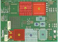
This article series describes initial test results for low-silver alloys using these solder paste alloy assessment protocols for BGAs and leaded components, and the impact of the alloys on printed circuit assembly process windows. Specific pass/fail criteria for acceptance of an alloy are not included, however, as they may vary across industry segments. The assessment evaluates wetting behavior, solder joint thermal fatigue and mechanical shock reliability, intermetallic formation, general physical joint acceptability, and copper dissolution. The variables include multiple component types: two BGA components with the same paste/ball alloy combinations, and numerous leaded components that include common component platings.
Surface mount (SMT) process temperature windows are typically constrained on the low end by the ability to melt solder and form acceptable joints, and on the high end by the maximum process temperatures of other materials, such as components. These two constraints have led to a process window of approximately 25°C when soldering with more conventional, Sn-3.0Ag-0.5Cu paste. Low-silver SMT alloys have been found to reduce the thermal process window even further.
Background
During the industry transition from Sn-Pb to Pb-free solder in the early 2000s, significant work was performed by the iNEMI consortium to develop assembly process limits to both produce acceptable solder joints as well as protect other materials from damage. This work was originally presented at ECTC 2005. This presentation defined the characteristics of the acceptable process window for process alloys in the range of SAC305-SAC405 (Sn 3.0-4.0Ag 0.5Cu). It mandates that each and every solder joint has to reach at least 230°C during reflow to produce acceptable and reliable joints. In addition, this previous work defined the minimum peak temperature for SAC305 as 230-232°C, but theorized that low-Ag alloys may only increase that temperature by 5-7 degrees Celsius.
Solder alloys used in Surface Mount Technology (SMT) will generally require lower liquidus temperatures than those alloys used in wave soldering. SMT process temperature windows are typically constrained on the low end by the ability of the solder to melt and form good joints, and on the high end by the maximum exposure temperatures of the other materials, such as components or laminates. These two constraints have led to a process window of approximately 25°C with more conventional, Sn-3.0Ag-0.5Cu paste. Low-silver SMT alloys have been found to reduce the thermal process window even further. While the liquidus temperature is the theoretical minimum peak temperature that any solder joint must reach to start the wetting process, it is well known that this temperature is not always sufficient to produce acceptable joints on the various component plating surfaces. In addition, non-eutectic alloys remain pasty for several degrees and will often not produce acceptable joints until fully molten. It is therefore important to determine a minimum peak temperature at which a specific low-Ag alloy will repeatedly produce acceptable joints across the range of likely component sizes, platings, and PCB surface finishes. This minimum peak, or superheat, temperature is often 10-15°C higher than the liquidus point of the alloy. Superheat is defined as the temperature necessary to dissolve native oxides of metals, which is higher than the liquidus temperature. For low-silver reflow alloys with liquidus temperatures of 225-228°C, this produces a theoretical minimum peak of 240°C or higher. Extending the time above liquidus is sometimes used to improve solder joint formation but can cause increased intermetallic formation.
Maximum component temperatures, which define the upper limit of a process window, are often defined by the supplier, but in-lieu of clear limits the J-STD-020 classification requirements, based on package size, are typically used. Table 4-2 of the J-STD-020 will define the maximum peak component temperature for any given package on a PCA (Printed Circuit Assembly), with typical PCAs containing a range of components. The range of maximum package temperatures is between 245°C and 260°C. Many PCA designs contain a wide range of component sizes creating complexity in reflow oven program generation. It is typical to use the largest component to set the maximum peak temperature for a reflow profile, as it will typically be the coolest part of the board. Using Table 4-2 to define the maximum temperature for a large package will create a minimum peak temperature as high as 245°C.
An additional complication is the need to reach this minimum peak temperature at every solder joint across the entire PCA. Even with sophisticated reflow ovens, it is often difficult to keep the temperature delta across a complex or thermally massive PCA within 15°C.
The data presented here (see Table 1) is based on four low-Ag alloys’ data submitted by multiple alloy vendors over two years. These alloys are commercially available, and have different dopant concentrations. The next section details the test methods for alloy evaluation. The subsequent section details the test results.
Table 1: Liquidus temperatures of the alloys reviewed in this paper
Test Methods
The test protocol described below reflects the company’s standard evaluation procedure for reflow alloys for general electronics assembly use. For all of the tests the following were specified: industry standards and test boards where available, appropriate controls (an alloy currently used widely in production), test parameters and execution details. The tests address both reliability and manufacturability concerns when soldering with a low-Ag alloy.
Page 1 of 2
Share on:


Suggested Items
KYZEN to Focus on Aqueous Cleaning and Stencil Cleaning at SMTA Juarez
05/20/2025 | KYZEN'KYZEN, the global leader in innovative environmentally responsible cleaning chemistries, will exhibit at the SMTA Juarez Expo and Tech Forum, scheduled to take place Thursday, June 5 at the Injectronics Convention Center in Ciudad Jarez, Chihuahua.
Koh Young Installs 24,000th Inspection System at Top 20 EMS
05/14/2025 | Koh YoungKoh Young, the global leader in True 3D measurement-based inspection and metrology solutions, proudly announces the installation of its 24,000th inspection system at a Top 20 Global EMS in Thailand.
Indium’s Karthik Vijay to Present on Dual Alloy Solder Paste Systems at SMTA’s Electronics in Harsh Environments Conference
05/06/2025 | Indium CorporationIndium Corporation Technical Manager, Europe, Africa, and the Middle East Karthik Vijay will deliver a technical presentation on dual alloy solder paste systems at SMTA’s Electronics in Harsh Environments Conference, May 20-22 in Amsterdam, Netherlands.
SolderKing Achieves the Prestigious King’s Award for Enterprise in International Trade
05/06/2025 | SolderKingSolderKing Assembly Materials Ltd, a leading British manufacturer of high-performance soldering materials and consumables, has been honoured with a King’s Award for Enterprise, one of the UK’s most respected business honours.
Knocking Down the Bone Pile: Gold Mitigation for Class 2 Electronics
05/07/2025 | Nash Bell -- Column: Knocking Down the Bone PileIn electronic assemblies, the integrity of connections between components is paramount for ensuring reliability and performance. Gold embrittlement and dissolution are two critical phenomena that can compromise this integrity. Gold embrittlement occurs when gold diffuses into solder joints or alloys, resulting in mechanical brittleness and an increased susceptibility to cracking. Conversely, gold dissolution involves the melting away of gold into solder or metal matrices, potentially altering the electrical and mechanical properties of the joint.