-

- News
- Books
Featured Books
- smt007 Magazine
Latest Issues
Current Issue
What's Your Sweet Spot?
Are you in a niche that’s growing or shrinking? Is it time to reassess and refocus? We spotlight companies thriving by redefining or reinforcing their niche. What are their insights?

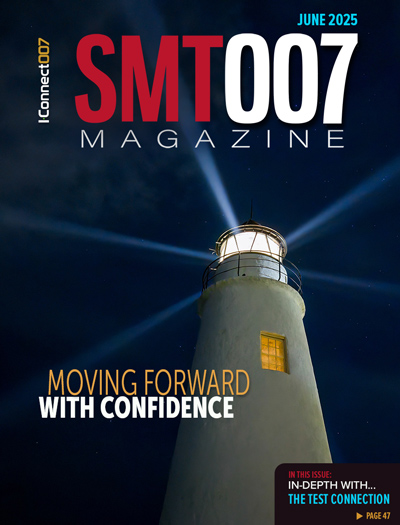
Moving Forward With Confidence
In this issue, we focus on sales and quoting, workforce training, new IPC leadership in the U.S. and Canada, the effects of tariffs, CFX standards, and much more—all designed to provide perspective as you move through the cloud bank of today's shifting economic market.

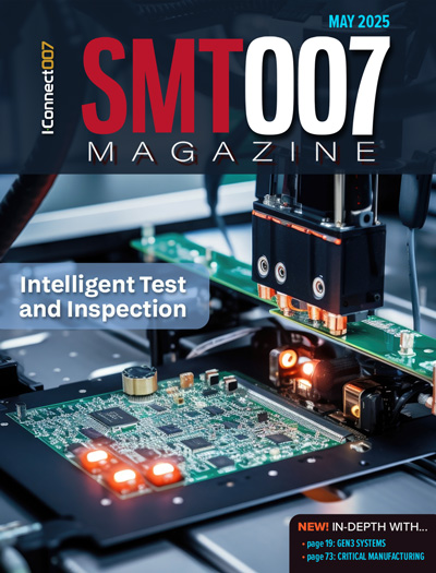
Intelligent Test and Inspection
Are you ready to explore the cutting-edge advancements shaping the electronics manufacturing industry? The May 2025 issue of SMT007 Magazine is packed with insights, innovations, and expert perspectives that you won’t want to miss.
- Articles
- Columns
- Links
- Media kit
||| MENU - smt007 Magazine
ESCATEC Solves Problem of Overheating High Brightness LEDs
September 7, 2015 | ESCATECEstimated reading time: 1 minute
ESCATEC, one of Europe's leading providers of contract design and manufacturing services, will be launching its solution to the challenge of effectively cooling high brightness LEDs on its stand E8 at the LED Professional Symposium 2015 in Bregenz, Austria on 22-24 September 2015.
ESCATEC's Heat Spreader solution solders the LEDs onto a copper substrate, which is up to ten times more effective at dissipating the heat generated by the LEDs than current solutions. The CoolRunning design means that LEDs with a power density of up to 10W per mm2 could be passively cooled.
The Heat Spreader was developed in response to a customer visit to ESCATEC's FutureLab where novel and innovative solutions are developed for LED applications. "Heat dissipation is always a challenge for LEDs as their compact size means that the LEDs can be packed close together to form a powerful illumination source but that also forms a highly concentrated heat source, for example, when a hundred 5 Amp LEDs are side by side," explained Wolfgang Plank, Manager of the FutureLab. "Our novel Heat Spreader solution opens up compact, high power LEDs of, say 1000W, to be used in many new applications such as stage lighting, architectural illumination and video projectors."
By starting from the bare LED die, ESCATEC can customise the solution with regards to the size of the package, the shape of the beam so that there are minimal losses, and the wavelength of the light along with its intensity. This freedom of design enables the LED solution to be highly efficient, appropriately cooled and optimised for the required power consumption. It also enables the lens or lens array to be custom made to provide the exact optics required by the application and ensures that design can be compact with high optical efficiency.
About ESCATEC
The ESCATEC Group provides fully-integrated electronic and mechatronic design and manufacturing solutions to assist customers in achieving success in their market. Its one-stop solutions and best-in-class service enable companies around the world to operate more profitably, sustainably and efficiently. Founded in 1984, its history is full of innovation, which made it a first choice partner for many European and North American OEMs. The Swiss-owned company perfectly blends Swiss business philosophy and attention to quality, precision and detail with the advantage of low-cost, mass-volume manufacturing capabilities in its Asian factories.
Suggested Items
Trouble in Your Tank: Can You Drill the Perfect Hole?
07/07/2025 | Michael Carano -- Column: Trouble in Your TankIn the movie “Friday Night Lights,” the head football coach (played by Billy Bob Thornton) addresses his high school football team on a hot day in August in West Texas. He asks his players one question: “Can you be perfect?” That is an interesting question, in football and the printed circuit board fabrication world, where being perfect is somewhat elusive. When it comes to mechanical drilling and via formation, can you drill the perfect hole time after time?
The Evolution of Picosecond Laser Drilling
06/19/2025 | Marcy LaRont, PCB007 MagazineIs it hard to imagine a single laser pulse reduced not only from nanoseconds to picoseconds in its pulse duration, but even to femtoseconds? Well, buckle up because it seems we are there. In this interview, Dr. Stefan Rung, technical director of laser machines at Schmoll Maschinen GmbH, traces the technology trajectory of the laser drill from the CO2 laser to cutting-edge picosecond and hybrid laser drilling systems, highlighting the benefits and limitations of each method, and demonstrating how laser innovations are shaping the future of PCB fabrication.
Day 2: More Cutting-edge Insights at the EIPC Summer Conference
06/18/2025 | Pete Starkey, I-Connect007The European Institute for the PCB Community (EIPC) summer conference took place this year in Edinburgh, Scotland, June 3-4. This is the third of three articles on the conference. The other two cover Day 1’s sessions and the opening keynote speech. Below is a recap of the second day’s sessions.
Day 1: Cutting Edge Insights at the EIPC Summer Conference
06/17/2025 | Pete Starkey, I-Connect007The European Institute for the PCB Community (EIPC) Summer Conference took place this year in Edinburgh, Scotland, June 3-4. This is the second of three articles on the conference. The other two cover the keynote speeches and Day 2 of the technical conference. Below is a recap of the first day’s sessions.
Preventing Surface Prep Defects and Ensuring Reliability
06/10/2025 | Marcy LaRont, PCB007 MagazineIn printed circuit board (PCB) fabrication, surface preparation is a critical process that ensures strong adhesion, reliable plating, and long-term product performance. Without proper surface treatment, manufacturers may encounter defects such as delamination, poor solder mask adhesion, and plating failures. This article examines key surface preparation techniques, common defects resulting from improper processes, and real-world case studies that illustrate best practices.


