-
- News
- Books
Featured Books
- pcb007 Magazine
Latest Issues
Current IssueSales: From Pitch to PO
From the first cold call to finally receiving that first purchase order, the July PCB007 Magazine breaks down some critical parts of the sales stack. To up your sales game, read on!
The Hole Truth: Via Integrity in an HDI World
From the drilled hole to registration across multiple sequential lamination cycles, to the quality of your copper plating, via reliability in an HDI world is becoming an ever-greater challenge. This month we look at “The Hole Truth,” from creating the “perfect” via to how you can assure via quality and reliability, the first time, every time.
In Pursuit of Perfection: Defect Reduction
For bare PCB board fabrication, defect reduction is a critical aspect of a company's bottom line profitability. In this issue, we examine how imaging, etching, and plating processes can provide information and insight into reducing defects and increasing yields.
- Articles
- Columns
- Links
- Media kit
||| MENU - pcb007 Magazine
Rainbow Technology Systems to Launch Unique Singulation System at Productronica
October 12, 2015 | Rainbow Technology SystemsEstimated reading time: 2 minutes
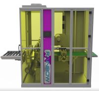
Rainbow Technology Systems, the company which brought the revolutionary Rainbow Process PCB production system to the electronics sector, is to introduce a unique Singulation System for use with digital imaging systems at this year’s Productronica exhibition.
The Rainbow Singulation System is a fully automated coating and laminating machine that takes a copper panel, cleans it, coats it both sides with solvent-free etch resist and laminates it with a thin layer of mylar. The edges of the panel are then sealed with UV light and panels are ejected ready for imaging in a digital imaging machine such as LDI or DMD.
Key to the process is Rainbow’s patented solvent-free etch resist which remains in a liquid state after coating. This removes the need for an oven as there is no solvent to release. The resist coating is thin ( <8 µm) and protected by mylar plus the machine automatically seals around the edge of each panel to offer easy, safe handling.
A key advantage of the system is that it will allow far faster throughput through a digital imaging machine as the Rainbow resist is much easier and faster to cure than dryfilm. After imaging, the mylar is peeled off and the panel goes through the develop, etch and strip stages in the same way as a dryfilm panel. As the thin coating and liquid state of the uncured resist allows faster developing, etching and stripping than normal it means the existing etch equipment can clear out higher density circuits (finer track and gap).
Jonathan Kennett, CEO, Rainbow Technology Systems said: “Our whole purpose at Rainbow is to find innovative ways of making the electronics production process easier, more efficient and more profitable. The new Singulation System achieves these aims for manufacturers using laser direct imaging equipment for PCB production.”
“We have spent many years to develop and refine the chemistry used in the solvent-free resist which is at the core of the cost and efficiency savings in the new system. This is the first significant change in the formulation of resist in the past 30 years so it is truly revolutionary, ” he added.
About Rainbow Technology Systems
The technology behind the Rainbow Singulation System is the brainchild of chief executive and founder Jonathan Kennett who set up Rainbow Technology Systems in 2005 to develop fine line printing technologies for the PCB market. Jonathan pioneered the development of contact cleaning technology for the electronics and high-tech sectors 25 years ago when he founded Teknek which has become the global leader in contact cleaning and yield improvement equipment. Other founder members of the senior management team include John Cunningham (chief chemist) and Robert Gibson (chief mechanical designer).
Suggested Items
I-Connect007 Editor’s Choice: Five Must-Reads for the Week
07/18/2025 | Nolan Johnson, I-Connect007It may be the middle of the summer, but the news doesn’t quit, and there’s plenty to talk about this week, whether you’re talking technical or on a global scale. When I have to choose six items instead of my regular five, you know it’s good. I start by highlighting my interview with Martyn Gaudion on his latest book, share some concerning tariff news, follow that up with some promising (and not-so-promising) investments, and feature a paper from last January’s inaugural Pan-European Design Conference.
Elephantech Launches World’s Smallest-Class Copper Nanofiller
07/17/2025 | ElephantechJapanese deep-tech startup Elephantech has launched its cutting-edge 15 nm class copper nanofiller – the smallest class available globally. This breakthrough makes Elephantech one of the first companies in the world to provide such advanced material for commercial use.
Copper Price Surge Raises Alarms for Electronics
07/15/2025 | Global Electronics Association Advocacy and Government Relations TeamThe copper market is experiencing major turbulence in the wake of U.S. President Donald Trump’s announcement of a 50% tariff on imported copper effective Aug. 1. Recent news reports, including from the New York Times, sent U.S. copper futures soaring to record highs, climbing nearly 13% in a single day as manufacturers braced for supply shocks and surging costs.
I-Connect007 Editor’s Choice: Five Must-Reads for the Week
07/11/2025 | Andy Shaughnessy, Design007 MagazineThis week, we have quite a variety of news items and articles for you. News continues to stream out of Washington, D.C., with tariffs rearing their controversial head again. Because these tariffs are targeted at overseas copper manufacturers, this news has a direct effect on our industry.I-Connect007 Editor’s Choice: Five Must-Reads for the Week
Digital Twin Concept in Copper Electroplating Process Performance
07/11/2025 | Aga Franczak, Robrecht Belis, Elsyca N.V.PCB manufacturing involves transforming a design into a physical board while meeting specific requirements. Understanding these design specifications is crucial, as they directly impact the PCB's fabrication process, performance, and yield rate. One key design specification is copper thieving—the addition of “dummy” pads across the surface that are plated along with the features designed on the outer layers. The purpose of the process is to provide a uniform distribution of copper across the outer layers to make the plating current density and plating in the holes more uniform.