

















 The Fearless Connector: Why I Chose the Hard Road
 The Clean Truth: The Clean Truth About No-Clean Flux
 Global Sourcing Spotlight: Beyond China Plus One—Building a Truly Global Supply Network






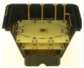
We have planned to take a closer look at the soldering process with vacuum profiles and therefore an evaluation project had been performed. As a result of the uniform distribution of the vapor during the pre-vacuum phase, it was possible to significantly improve the three-dimensional soldering process for a MID (molded interconnect device) application. Here you will find some of the obtained results.
The use of MID technology
MID technology is used in particular where significant miniaturization, freedom of design with regard to geometry, and a reduced number of components for the electronics assembly is required. The electrical and mechanical features, which are normally distributed to various components during conceptualization and development, are combined into a single MID part.
An intelligent, energy-self-sufficient pressure sensor system with a MID housing was recently developed as part of the Joint Project for Intelligent, energy-self-sufficient couplings for fluidic systems for automotive applications of the German Federal Ministry of Education and Research (No. V3EAAS010). Figure 1 (left) shows the individual process steps required for the LPKF-LDS technology in the production of the interconnect device. With the MID housing, the sensor could be made in a very compact manner and with a reduced number of components.
Due to the three-dimensional design of the housing, the contact points between the interconnect device and the PCBs are vertically distributed (see Figure 1, right). As shown in Figure 2, the package was soldered in the worst possible position for vapor phase soldering, namely as a cup.
Figure 2: Positioning of the thermocouples and alignment of the MID housing (left), and measured temperature profiles (right) during vapor phase soldering only with main vacuum.
In conventional systems, this type of component positioning leads to excessive carry-over of the vapor phase medium. This results in some solder joints being heated more quickly than others, loss of medium from the system due to the cup effect – and a negative influence on the soldering profile. In order to investigate this effect, a soldering test was first of all conducted using a standard vapor phase process with a lead-free temperature profile.
Vapor phase process without pre-vacuum, soldering test
As shown in Figure 2 (left), thermocouples are attached to various internal mounting levels, as well as to the upper and lower edges of the housing. First of all, the temperature profiles were recorded on the component while injecting the Galden at ambient pressure and followed by the main vacuum. The curves in Figure 2 (right) make it apparent that the measurement results demonstrate considerable differences with regard to heat up times. The great differences observed with regard to the heat transfer on the component can be traced back to two causes: on the one hand, the vapor rising up from the bottom to top causes time-delayed heat energy input over the height of the housing and, on the other hand, the air from the lowermost areas cannot be fully displaced. These two effects influence the development of the temperature gradient over time, and thus the heat up behavior of the component as well.
Vapor phase process with pre-vacuum, soldering test
The next step of experimental investigation involved testing with the same component alignment and thermocouples positioning and the addition of a pre-vacuum step. Right from the very beginning of the soldering process, a pre-vacuum of 100 mbar was pulled and Galden was directly injected into the vacuum. The measurement results depicted in Figure 3 reveal a much more uniform temperature rise at various locations on the component, which enable a much more uniform transition into the liquidus phase at various component mounting levels.
Figure 3: Measured temperature profiles at various locations on the component during vapor phase soldering with pre vacuum and main vacuum.
Page 1 of 2


