


 Nolan’s Notes: Finding Your Sweet Spot
 Standard of Excellence: Delivering Excellence—A Daily Goal
 Knocking Down the Bone Pile: Tin Whisker Mitigation in Aerospace Applications, Part 3


MIRTEC to Exhibit the All New MV-6 OMNI at productronica
October 22, 2015 | MirtecEstimated reading time: 2 minutes
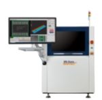
MIRTEC, “The Global Leader in Inspection Technology,” will premier the technologically advanced MV-6 OMNI 3D Series in Hall A2, Stand 139 at the upcoming Productronica international trade fair, scheduled to take place November 10-13, at the Messe in Munich, Germany.
The new high-speed, high-performance 3D AOI machine boasts 15 mega pixel CoaXPress camera technology, as well as advanced eight phase color lighting system. The machine includes a ten micron/pixel prevision telecentric compound lens design, integrated ten mega pixel side-viewer camera system, and a precision closed loop AC servo drive motor system.
The MV-6 OMNI has extremely simple programming and operation, and is priced at under €100k (while supplies last).
Also on display will be Mirtec’s flagship, the MV-9 AOI system, which achieves the highest productivity and ultimate inspection performance, falls calls will be avoided. For the 3D measurement the MV-9 system is working with the "Shadow Free" Moiré Phase Shift image processing. Additionally it is equipped with the 6 Phase colour lighting system for an optimized recognition of lifted leads. At the show, the MV-9 will be linked to a YXLON Cheetah with SmartLoop.
The MV-9 utilizes a high resolution digital 15 MP camera technology with telecentric lens. The four 10 MP side cameras (Side-Viewer®) offer a spacial test and provide valuable information for a secure and reliable detection of side defects. Also, the inspection of complex components is greatly enhanced. The MV-9 is now also available with a 25 MP camera and 7.7 µm lens for components down to 03015.
Also on display will be the MS-15 In-Line SPI System. It also uses the shadow free Moiré Phase Shift Imaging technology to inspect solder paste depositions on PCBs post screen print for insufficient or excessive solder, shape deformity, shift of deposition and bridging. The MS-15 uses the same high precision platform as MIRTEC’s MV-9 Series.
Both systems, the MV-9 and the MS-15, can additionally be equipped with the new CoaXPress which leads to an increase of inspection speed of around 25% compared to the standard camera technology. CoaXPress combines the simplicity of coaxial cable with state of the art high speed serial data technology. The combination of these two features provides a revolutionary leap forward in high speed image and data transmission.
The MV-3 Desktop AOI System has been designed to automatically inspect for manufacturing defects both pre and post reflow. The MV-3 systems offer superior fault coverage and will detect defects such as component presence/absence, polarity, miss alignment, insufficient solder, solder bridging, etc. The system software is very powerful yet extremely simple to use. With its perfect cost-performance ratio this system addresses especially companies with small and medium productions.
Finally, stop by Hall A4, Stand 506 to see an MS-11 and MV-7OMNI linked to the YXLON Cheetah X-ray system showing SmartLoop.
For more information, or to schedule a demo, contact your Mirtec sales representative or stop by Hall A2, Stand 139, or Hall A4, Stand 506 at Productronica.
Share on:


Suggested Items
Driving Innovation: Direct Imaging vs. Conventional Exposure
07/01/2025 | Simon Khesin -- Column: Driving InnovationMy first camera used Kodak film. I even experimented with developing photos in the bathroom, though I usually dropped the film off at a Kodak center and received the prints two weeks later, only to discover that some images were out of focus or poorly framed. Today, every smartphone contains a high-quality camera capable of producing stunning images instantly.
Hands-On Demos Now Available for Apollo Seiko’s EF and AF Selective Soldering Lines
06/30/2025 | Apollo SeikoApollo Seiko, a leading innovator in soldering technology, is excited to spotlight its expanded lineup of EF and AF Series Selective Soldering Systems, now available for live demonstrations in its newly dedicated demo room.
Indium Corporation Expert to Present on Automotive and Industrial Solder Bonding Solutions at Global Electronics Association Workshop
06/26/2025 | IndiumIndium Corporation Principal Engineer, Advanced Materials, Andy Mackie, Ph.D., MSc, will deliver a technical presentation on innovative solder bonding solutions for automotive and industrial applications at the Global Electronics A
Fresh PCB Concepts: Assembly Challenges with Micro Components and Standard Solder Mask Practices
06/26/2025 | Team NCAB -- Column: Fresh PCB ConceptsMicro components have redefined what is possible in PCB design. With package sizes like 01005 and 0201 becoming more common in high-density layouts, designers are now expected to pack more performance into smaller spaces than ever before. While these advancements support miniaturization and functionality, they introduce new assembly challenges, particularly with traditional solder mask and legend application processes.
Knocking Down the Bone Pile: Tin Whisker Mitigation in Aerospace Applications, Part 3
06/25/2025 | Nash Bell -- Column: Knocking Down the Bone PileTin whiskers are slender, hair-like metallic growths that can develop on the surface of tin-plated electronic components. Typically measuring a few micrometers in diameter and growing several millimeters in length, they form through an electrochemical process influenced by environmental factors such as temperature variations, mechanical or compressive stress, and the aging of solder alloys.