


 Nolan’s Notes: Finding Your Sweet Spot
 Standard of Excellence: Delivering Excellence—A Daily Goal
 Knocking Down the Bone Pile: Tin Whisker Mitigation in Aerospace Applications, Part 3


Saki Presents 'From Inspection to Measurement' at Productronica, Stand A2.239
November 3, 2015 | Saki CorporationEstimated reading time: 2 minutes
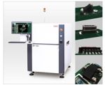
Saki Corporation, an innovator in the field of automated optical inspection equipment, announces that its new 3D automated optical inspection, solder paste, and x-ray technology and equipment will be demonstrated at Productronica 2015, in Stand A2.239, as part of the theme "From Inspection to Measurement."
"To truly capture all the potential problems and failures in circuit boards today, it requires a combination of the correct lighting, type of camera, camera angles, and the ability to not just inspect, but also to measure in true 3D," explained Katsuhiro (Eddie) Ichiyama, general manager of Saki Europe, GmbH. "Other considerations are the ease of programming and whether you can do it off-line with a system that can simulate the machine or if you will have to factor in production down-time for programming. Our products, combined with over 20 years of expertise, can truly capture all the potential problems and failures in circuit boards today. During Productronica, our technical experts will be available to help companies understand how to meet their inspection needs and challenges."
Several new 3D automated in-line x-ray, solder paste, and optical inspection systems will be on display at Productronica, including Saki's newest line of 3D in-line automated optical inspection systems. This 3D product line has a newly designed gantry, in 3 configurations and sizes, with a dual-lane model and a 3D scanning head with side camera option. Saki's AOI system doesn't just inspect, it provides measurements for components with a height range between 0 and 20mm and does it with 1-micron height resolution, a false call rate of less than 100 ppm with 0 escapes, and the fastest 3D AOI speed on the market with an average takt time of 18 seconds. It captures the most difficult defects, such as lifted leads, tombstones, reverses, and height variations.
Productronica 2015 is being held in Munich, Germany, from November 10-13, 2015. Visit stand A2.239 to find out more, or for more information contact Saki in the US at +1-510-623-SAKI (+1-510-623-7254), email sales.us@sakicorp.com or in Europe at +49 89 309 04 69-0, email saki.eu@sakicorp.com, or visit our website at www.sakicorp.com.
About Saki Corporation
Since its inception in 1994, Saki has led the way in the development of automatic recognition through robotic vision technology, applying ground-breaking image processing tools to solve inspection problems associated with printed circuit board assembly. Saki Corporation has headquarters in Tokyo, Japan with offices and sales and support centers around the world. Saki has Quality Management System JIS Q 9001:2008 and ISO 9001:2008 certifications.
Share on:


Suggested Items
Driving Innovation: Direct Imaging vs. Conventional Exposure
07/01/2025 | Simon Khesin -- Column: Driving InnovationMy first camera used Kodak film. I even experimented with developing photos in the bathroom, though I usually dropped the film off at a Kodak center and received the prints two weeks later, only to discover that some images were out of focus or poorly framed. Today, every smartphone contains a high-quality camera capable of producing stunning images instantly.
Hands-On Demos Now Available for Apollo Seiko’s EF and AF Selective Soldering Lines
06/30/2025 | Apollo SeikoApollo Seiko, a leading innovator in soldering technology, is excited to spotlight its expanded lineup of EF and AF Series Selective Soldering Systems, now available for live demonstrations in its newly dedicated demo room.
Indium Corporation Expert to Present on Automotive and Industrial Solder Bonding Solutions at Global Electronics Association Workshop
06/26/2025 | IndiumIndium Corporation Principal Engineer, Advanced Materials, Andy Mackie, Ph.D., MSc, will deliver a technical presentation on innovative solder bonding solutions for automotive and industrial applications at the Global Electronics A
Fresh PCB Concepts: Assembly Challenges with Micro Components and Standard Solder Mask Practices
06/26/2025 | Team NCAB -- Column: Fresh PCB ConceptsMicro components have redefined what is possible in PCB design. With package sizes like 01005 and 0201 becoming more common in high-density layouts, designers are now expected to pack more performance into smaller spaces than ever before. While these advancements support miniaturization and functionality, they introduce new assembly challenges, particularly with traditional solder mask and legend application processes.
Knocking Down the Bone Pile: Tin Whisker Mitigation in Aerospace Applications, Part 3
06/25/2025 | Nash Bell -- Column: Knocking Down the Bone PileTin whiskers are slender, hair-like metallic growths that can develop on the surface of tin-plated electronic components. Typically measuring a few micrometers in diameter and growing several millimeters in length, they form through an electrochemical process influenced by environmental factors such as temperature variations, mechanical or compressive stress, and the aging of solder alloys.