


















 It’s Only Common Sense: When the Cheapest Board Becomes the Most Expensive
 The Chemical Connection: Employee and Operator Empowerment in the Age of AI
 The Big Picture: Not One, But Three Grey Rhinos





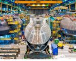
The full contract covers the design and remaining build, test and commissioning activities on Anson, the fifth of seven technologically-advanced submarines in the class. Manufacturing commenced in 2010. Anson is now at an advanced stage of construction at our Barrow-in-Furness, Cumbria site and on schedule to leave for sea trials in 2020.
Tony Johns, Managing Director of BAE Systems Submarines, said: "Signing this contract is an important milestone in the Astute programme.
"This is a hugely complex national endeavour and we are proud of the role we play in helping to protect our nation's interests.
"HMS Astute and HMS Ambush are already demonstrating their world-class capabilities with the Royal Navy, whilst the third submarine in the class, Artful, is continuing with her sea trials. The build phase for the fourth, Audacious, is also well advanced, so we continue to make positive progress across the programme."
The contract was announced by Philip Dunne MP, Minister of State for Defence Procurement, during a visit to our Company today.
He said: “This £1.3 billion contract marks an important step in the progress of the Astute programme. This is a key part of our £166 billion plan to ensure that our armed forces have the equipment they need to defend the UK’s interests across the seas, in the skies and on land, both at home and abroad.”
“This new contract for Anson not only provides significant financial savings of £50 million to the taxpayer but also secures thousands of jobs in Barrow and across the UK supply chain, demonstrating the Government’s commitment to increase defence spending each year for the rest of the decade.”
We employ more than 7,600 people in our Submarines business, including those working on the Astute programme. Boat six Agamemnon and the yet-to-be named seventh are also under construction in Barrow.
Astute class submarines mark a step change in defence capability. Powered by a nuclear-reactor, each of the submarines will provide land strike, strategic intelligence-gathering, anti-submarine and surface ship warfare capabilities.
We are also leading the design phase on the programme to replace the current fleet of Vanguard submarines, which carry the UK's strategic national deterrent.
In readiness for the start of construction on this programme, our site is undergoing significant redevelopment with new facilities to be built alongside the refurbishment of others.


