


 Knocking Down the Bone Pile: Revamp Your Components with BGA Reballing
 SMT Perspectives & Prospects: Artificial Intelligence Part 6: Data Module 1
 Standard of Excellence: Overcoming Service Failures—The Art of the Apology


Akrometrix LLC Debuts AKM600P - FOWLP Panel Warpage Measurement System
December 3, 2015 | Akrometrix LLCEstimated reading time: 1 minute
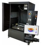
Akrometrix LLC, a leading provider of thermal warpage and strain metrology equipment to both the front- and back-end semiconductor and electronics industries, today announced the company’s entry into the Fan Out Wafer Level Processing (FOWLP) market with an innovative, single shot full field of view warpage metrology system for panels up to 600 x 600 mm.
Scalable manufacturing technology is driving the industry’s need to move from wafer sized limitations in the FOWLP market to panel based manufacturing. This is a logical step to move beyond wafers to panel sized substrates, which have been used in the LCD industry for years.
Akrometrix’s AKM600P warpage measurement system enables customers to complete single shot warpage measurement of the entire panel and individual die on panels up to 600 x 600 mm simultaneously. The complete measurement and analysis of a panel of this size provides z-resolution down to 1.25 µm and takes less than two seconds to complete using the patented Shadow Moiré technology. Additionally, warpage measurements can be conducted at room temperature or up to 300°C for those needing thermal profiles.
“Akrometrix’s Shadow Moiré systems have become the industry standard for warpage measurement, especially at temperature,” noted Mayson Brooks, Akrometrix’s President and CEO. “With the emerging market for FOWLP in panel form, our technology is uniquely positioned to scale up to panel sized warpage measurements, sacrificing neither warpage resolution nor measurement acquisition time in moving from die size measurements to 600 x 600 mm measurements. The ability to measure both wafers and panels on the same equipment is the perfect ‘bridge’ tool as customers continue to do wafer processing while developing their panel technology.”
Share on:


Testimonial
"Our marketing partnership with I-Connect007 is already delivering. Just a day after our press release went live, we received a direct inquiry about our updated products!"
Rachael Temple - AlltematedSuggested Items
LPKF Joins productronica’s 50th Anniversary, Showcasing Laser Technology for Electronics Manufacturing
10/10/2025 | LPKF Laser & ElectronicsLPKF Laser & Electronics invites visitors to productronica 2025 in Munich from November 18 to 21. At booth 305 in hall B2, the company will present its portfolio of modern laser technologies for the electronics industry live – from prototyping systems and high-performance depaneling to laser plastic welding for electronic housings and thin glass processing for advanced packaging.
Marco Pieters Appointed ASML Chief Technology Officer
10/09/2025 | ASMLASML Holding NV (ASML) announced the appointment of Marco Pieters as Executive Vice President and Chief Technology Officer, reporting to President and Chief Executive Officer, Christophe Fouquet.
Advanced Rework Technology Inspires Students at National Manufacturing Day 2025
10/08/2025 | A.R.T. Ltd.Advanced Rework Technology Ltd. (A.R.T.), a leading independent IPC-accredited training provider, joined forces with Jaltek, a UK-based electronics manufacturer with over 35 years’ experience in designing and producing high-quality electronic products, to deliver hands-on workshops for students during National Manufacturing Day 2025.
I-Connect007 Releases Episode 5 of Groundbreaking Ultra HDI Podcast Series
10/10/2025 | I-Connect007In Episode 5 “Via Structures,” host Nolan Johnson welcomes back John Johnson, Director of Quality and Advanced Technology at American Standard Circuits. Together, they explore the designer’s perspective on UHDI’s impact on via structures, diving into the metallurgy, chemistry, mechanical considerations, and stackup reduction that provide greater design flexibility and fewer constraints than ever before.
EDADOC Ushers in a New Era of Robotics Innovation
10/07/2025 | Edy Yu, Editor-in-Chief, ECIOOn Sept. 11, Shanghai Zhiyuan Technology Co., Ltd. (MScape) made a stunning debut at Shanghai’s 2025 Fourth North Bund Cybersecurity Forum and Cyber Intelligence Security Frontier Technology and Equipment Exhibition. The company presented the world’s first Dvorak super heterogeneous architecture and the Zhijing T-series-embodied intelligence (robotics) edge computing power platform. This has been a game-changer in the cybersecurity technology field, filling the gap in the domestic robotics core computing power platform.