


 Knocking Down the Bone Pile: Revamp Your Components with BGA Reballing
 SMT Perspectives & Prospects: Artificial Intelligence Part 6: Data Module 1
 Standard of Excellence: Overcoming Service Failures—The Art of the Apology


SHENMAO Introduces 606-P133 Solder Paste for Laser Soldering
December 3, 2015 | SHENMAO America Inc.Estimated reading time: Less than a minute
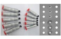
SHENMAO PF606-P133 Solder Paste is designed for selective laser soldering on tiny solder joints (1.5mm or smaller), especially on expensive, temperature–sensitive components and assemblies. In the past, such a small solder joint is not suitable for standard reflow processes and has to be soldered manually. With PF606-P133 Solder Paste, automatic laser soldering can easily be accomplished.
Within only several seconds of heating after dispensing, solder joint is well-formed with minimal flux residue and without splash or solder ball. Process time can be greatly reduced with extremely high yield rate.
PF606-P133 is approved by world leading electronic component manufacturers.
As the World’s Major Solder Materials Provider, SHENMAO produces SMT Solder Paste, Wave Solder Bar, Solder Wire and Flux, Solder Preforms, Semiconductor Packaging Solder Spheres, Wafer Bumping Solder Paste, Dipping Flux and PV Ribbon.
For more information, please contact:
SHENMAO America, Inc. www.shenmao.com; Tel: 408-943 -1755; e-mail: usa@shenmao.us
Share on:


Testimonial
"Our marketing partnership with I-Connect007 is already delivering. Just a day after our press release went live, we received a direct inquiry about our updated products!"
Rachael Temple - AlltematedSuggested Items
Knocking Down the Bone Pile: Revamp Your Components with BGA Reballing
10/14/2025 | Nash Bell -- Column: Knocking Down the Bone PileBall grid array (BGA) components evolved from pin grid array (PGA) devices, carrying over many of the same electrical benefits while introducing a more compact and efficient interconnect format. Instead of discrete leads, BGAs rely on solder balls on the underside of the package to connect to the PCB. In some advanced designs, solder balls are on both the PCB and the BGA package. In stacked configurations, such as package-on-package (PoP), these solder balls also interconnect multiple packages, enabling higher functionality in a smaller footprint.
Indium to Showcase High-Reliability Solder and Flux-Cored Wire Solutions at SMTA International
10/09/2025 | Indium CorporationAs one of the leading materials providers in the electronics industry, Indium Corporation® will feature its innovative, high-reliability solder and flux-cored wire products at SMTA International (SMTAI), to be held October 19-23 in Rosemont, Illinois.
‘Create your Connections’ – Rehm at productronica 2025 in Munich
10/08/2025 | Rehm Thermal SystemsThe electronics industry is undergoing dynamic transformation: smart production lines, sustainability, artificial intelligence, and sensor technologies dominate current discussions.
Amplifying Innovation: New Podcast Series Spotlights Electronics Industry Leaders
10/08/2025 | I-Connect007In the debut episode, “Building Reliability: KOKI’s Approach to Solder Joint Challenges,” host Marcy LaRont speaks with Shantanu Joshi, Head of Customer Solutions and Operational Excellence at KOKI Solder America. They explore how advanced materials, such as crack-free fluxes and zero-flux-residue solder pastes, are addressing issues like voiding, heat dissipation, and solder joint reliability in demanding applications, where failure can result in costly repairs or even catastrophic loss.
SASinno Americas Introduces the Ultra Series
10/07/2025 | SASinno AmericasSASinno Americas has introduced the new Ultra Series, the latest generation of offline selective soldering systems. Available in two models—the Ultra-i1 and Ultra-i2—the new series is designed to meet the needs of manufacturers running small to medium batch sizes, multiple product types, and frequent line changes, while maintaining exceptional precision and process control.