













 Dan’s Biz Bookshelf: ‘Building a Story Brand 2.0’
 It’s Only Common Sense: Why Should They Take Your Call?





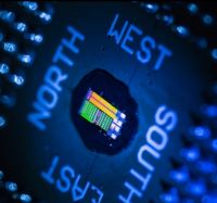
Using only processes found in existing microchip fabrication facilities, researchers at MIT, the University of California at Berkeley, and the University of Colorado have produced a working optoelectronic microprocessor, which computes electronically but uses light to move information.
Optical communication could dramatically reduce chips’ power consumption, which is not only desirable in its own right but essential to maintaining the steady increases in computing power that we’ve come to expect.
Demonstrating that optical chips can be built with no alteration to existing semiconductor manufacturing processes should make optical communication more attractive to the computer industry. But it also makes an already daunting engineering challenge even more difficult.
“You have to use new physics and new designs to figure out how you take ingredients and process recipes that are used to make transistors, and use those to make photodetectors, light modulators, waveguides, optical filters, and optical interfaces,” says MIT professor of electrical engineering Rajeev Ram, referring to the optical components necessary to encode data onto different wavelengths of light, transmit it across a chip, and then decode it. “How do you build all the optics using only the layers out of a transistor? It felt a bit like an episode of ‘MacGyver’ where he has to build an optical network using only old computer parts.”
The project began as a collaboration between Ram, Vladimir Stojanović, and Krste Asanovic, who were then on the MIT Department of Electrical Engineering and Computer Science faculty. Stojanović and Asanovic have since moved to Berkeley, and they, Ram, and Miloš A. Popović, who was a graduate student and postdoc at MIT before becoming an assistant professor of electrical engineering at Colorado, are the senior authors on a paper in Nature that describes the new chip.
They’re joined by 19 co-authors, eight of whom were at MIT when the work was done, including two of the four first authors: graduate students Chen Sun and Jason Orcutt, who has since joined IBM’s T. J. Watson Research Center.
Page 1 of 3
Share on:



Subscribe
Stay ahead of the technologies shaping the future of electronics with our latest newsletter, Advanced Electronics Packaging Digest. Get expert insights on advanced packaging, materials, and system-level innovation, delivered straight to your inbox.
Subscribe now to stay informed, competitive, and connected.
Suggested Items
REPORT: Closing the European Gap in Data Centre, Cloud, and AI Infrastructure Manufacturing
09/17/2026 | Global Electronics AssociationThe Global Electronics Association released From Chips to Systems: Building an End-to-End EU Strategy for Data Centre, Cloud Infrastructure and AI, a joint report with DECISION Études & Conseil. Europe is one of the world’s three largest markets for AI data centres.
Google to Invest €13 Billion in Finland AI Infrastructure Over Two Years
09/16/2026 | GoogleGoogle announced plans to invest at least €13 billion in digital infrastructure in Finland over the next two years (2027 - 2028), deepening its long-term commitment to the country and to Europe.
Data Center Power Demand to Rise 31% in 2026, Grid Gap to Widen in 2028
09/16/2026 | TrendForceTrendForce’s latest AI server industry research reports that CSPs are accelerating infrastructure deployments to meet surging demand for AI applications.
Closing the Gap: Measuring 20-µm Spacing in Advanced SiP Packaging
09/18/2026 | Axel Lindloff, Koh Young EuropeTwenty microns does not leave much room for error. As advanced packaging increases functional density, the distance between neighboring devices is shrinking to dimensions that create an entirely new set of inspection challenges. In some system-in-package (SiP) applications, components approximately 200 to 300 µm tall can be separated by gaps of only 20 to 30 µm. Measuring those spaces accurately requires considerably more than simply increasing camera magnification. The challenge is optical access.
Designing for a More ‘Intelligent’ and Connected Future
09/15/2026 | Marcy LaRont, I-Connect007 MagazineWith more collaborative and computationally demanding PCB designs, cloud-based workflows are rapidly moving from possibility to reality. But greater connectivity also raises new questions about data security, intellectual property, and the sharing of design information in an increasingly complex electronics ecosystem. In this interview, Kristin Moyer of the Global Electronics Association explores the benefits and challenges of cloud-based design environments, the growing importance of standardized data transfer protocols such as IPC-1751 and IPC-2581, and why a secure, intelligent data ecosystem will be essential for the future of co-design, automation, and advanced electronics manufacturing.