-

- News
- Books
Featured Books
- design007 Magazine
Latest Issues
Current Issue
Rules of Thumb
This month, we delve into rules of thumb—which ones work, which ones should be avoided. Rules of thumb are everywhere, but there may be hundreds of rules of thumb for PCB design. How do we separate the wheat from the chaff, so to speak?

Partial HDI
Our expert contributors provide a complete, detailed view of partial HDI this month. Most experienced PCB designers can start using this approach right away, but you need to know these tips, tricks and techniques first.

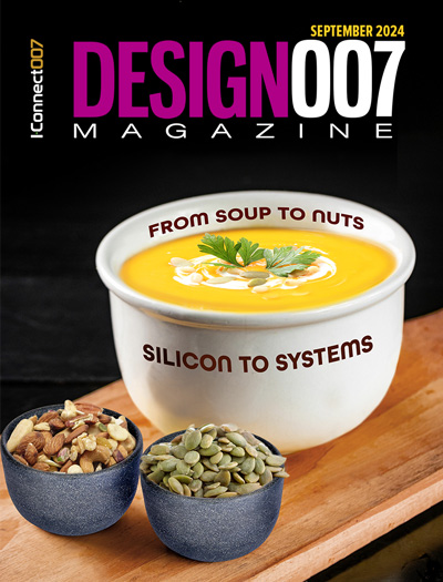
Silicon to Systems: From Soup to Nuts
This month, we asked our expert contributors to weigh in on silicon to systems—what it means to PCB designers and design engineers, EDA companies, and the rest of the PCB supply chain... from soup to nuts.
- Articles
- Columns
Search Console
- Links
- Media kit
||| MENU - design007 Magazine
Self-Stacking Nanogrids
January 22, 2016 | MITEstimated reading time: 4 minutes
Glass-like wires are not directly useful for electronic applications, but it might be possible to seed them with other types of molecules, which would make them electronically active, or to use them as a template for depositing other materials. The researchers hope that they can reproduce their results with more functional polymers. To that end, they had to theoretically characterize the process that yielded their results. “We use computer simulations to understand the key parameters controlling the polymer orientation,” Gadelrab says.
What they found was that the geometry of the cylinders in the bottom layer limited the possible orientations of the cylinders in the upper layer. If the walls of the lower cylinders are too steep to permit the upper cylinders from fitting in comfortably, the upper cylinders will try to find a different orientation.
It’s also important that the upper and lower layers have only weak chemical interactions. Otherwise, the upper cylinders will try to stack themselves on top of the lower ones like logs on a pile.
Both of these properties — cylinder geometry and chemical interaction — can be predicted from the physics of polymer molecules. So it should be possible to identify other polymers that will exhibit the same behavior.
According to Patrick Theofanis, an engineer at the chip manufacturer Intel, the nanocylinders themselves are less interesting than the spaces between them. “In general, the ability to pattern square holes is very useful for us,” he says.
“If you think of the back end of our chips, we have the back-end wiring, and then you have the interconnect layers between those back-end metal layers, and that’s where you’d like to be able to punch through holes and connect one layer to the next one. It’s an attractive technology because the aspect ratio is very tunable in the way that they’ve done their scheme.”
The research was funded by the National Science Foundation and the Taiwan Semiconductor Manufacturing Corporation.
Suggested Items
CHIPS for America Announces Up to $300M in Funding to Boost U.S. Semiconductor Packaging
11/21/2024 | U.S. Chamber of CommerceThe Biden-Harris Administration announced that the U.S. Department of Commerce (DOC) is entering negotiations to invest up to $300 million in advanced packaging research projects in Georgia, California, and Arizona to accelerate the development of cutting-edge technologies essential to the semiconductor industry.
Global Citizenship: What I’ve Learned About the American PCB Business
11/20/2024 | Tom Yang -- Column: Global CitizenshipNavigating the complexities of the American PCB business has been an eye-opening experience. During my time in America, I have become more familiar with the American PCB business and doing business here. If I may, and with your indulgence, I would like to share my humble impressions of the American PCB industry and the American way of doing business, which I find interesting and admirable.
Spirit Announces Purchase Agreement with Tex Tech Industries for Intended Sale of FMI
11/19/2024 | Spirit AeroSystems, Inc.Spirit AeroSystems Holdings, Inc. announces a purchase agreement to sell Fiber Materials, Inc (FMI) business based in Biddeford, Maine, and Woonsocket, Rhode Island, to Tex-Tech Industries, Inc. for $165,000,000 in cash, subject to customary adjustment.
Ventec to Become Primary PCB Materials Supplier for Teltonika
11/13/2024 | VentecVentec International Group and high-tech design and manufacturing company Teltonika announce that Ventec is to become supply chain partner and primary supplier of PCB base materials to Teltonika, which is preparing to open a new PCB manufacturing plant at its base in Vilnius, Lithuania.
AIM to Present on Micro/MiniLED Applications at Hangjia Talk in Shenzhen, China
11/11/2024 | AIM SolderAIM Solder, a leading global manufacturer of solder assembly materials for the electronics industry, is pleased to announce its participation in the upcoming Hangjia annual industry event focused on the future of the LED display sector.


