


 Flexible Thinking: Designing Flex Circuits for Dynamic Reliability
 Global PCB Connections: Rigid-flex and Flexible PCBs—The Backbone of Modern Electronics
 Happy’s Tech Talk #29: Bend-to-Install Semi-flex FR-4


Since the 1960s, computer chips have been built using a process called photolithography. But in the past five years, chip features have gotten smaller than the wavelength of light, which has required some ingenious modifications of photolithographic processes. Keeping up the rate of circuit miniaturization that we’ve come to expect — as predicted by Moore’s Law — will eventually require new manufacturing techniques.
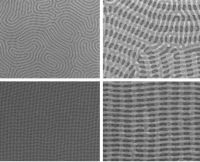
Block copolymers, molecules that spontaneously self-assemble into useful shapes, are one promising alternative to photolithography. In a new paper in the journal Nature Communications, MIT researchers describe the first technique for stacking layers of block-copolymer wires such that the wires in one layer naturally orient themselves perpendicularly to those in the layer below.
The ability to easily produce such “mesh structures” could make self-assembly a much more practical way to manufacture memory, optical chips, and even future generations of computer processors.
“There is previous work on fabricating a mesh structure — for example our work,” says Amir Tavakkoli, a postdoc in MIT’s Research Laboratory of Electronics and one of three first authors on the new paper. “We used posts that we had fabricated by electron-beam lithography, which is time consuming. But here, we don’t use the electron-beam lithography. We use the first layer of block copolymer as a template to self-assemble another layer of block copolymer on top of it.”
Tavakkoli’s co-first-authors on the paper are Sam Nicaise, a graduate student in electrical engineering, and Karim Gadelrab, a graduate student in materials science and engineering. The senior authors are Alfredo Alexander-Katz, the Walter Henry Gale Associate Professor of Materials Science and Engineering; Caroline Ross, the Toyota Professor of Materials Science and Engineering; and Karl Berggren, a professor of electrical engineering.
Page 1 of 3
Share on:


Testimonial
"The I-Connect007 team is outstanding—kind, responsive, and a true marketing partner. Their design team created fresh, eye-catching ads, and their editorial support polished our content to let our brand shine. Thank you all! "
Sweeney Ng - CEE PCBSuggested Items
Getters for Hermetic Packages: Mechanisms, Reliability Impact, and MacDermid Alpha Electronics Solutions
06/11/2026 | Michael Previti, MacDermid Alpha Electronics SolutionsHermetic packages protect chips, lasers, and sensors from the outside world, but the cavity inside can still change after seal. Small amounts of water, hydrogen, carbon dioxide, and organic vapor may remain after build or may form later from adhesives, films, and other internal materials. Getters reduce that risk by creating a planned sink for those gases inside the package. When teams choose the right getter early, they hold the headspace steady, cut reliability escapes, and lower the life-cycle cost of a high-value device.
Applied Materials Expands Singapore Manufacturing to Support AI Chip Demand
06/11/2026 | Applied MaterialsApplied Materials, Inc., the leader in materials engineering solutions for the semiconductor industry, has expanded its manufacturing and R&D operations in Singapore to support the global build-out of AI infrastructure.
Getters, Thermal Management, and High-Reliability Packaging: What’s Ahead in the Next Issue of Advanced Electronics Packaging Digest
06/10/2026 | I-Connect007The upcoming issue of Advanced Electronics Packaging Digest explores several technologies shaping the future of advanced packaging, from maintaining stable environments inside hermetic packages to managing heat in increasingly complex 3D architectures. The issue also examines packaging innovations for aerospace, defense, and automotive applications, as well as broader connections between semiconductor interconnects and the systems they support.
Below the Surface: From Nanometers to 10-Gauge—It’s More Than Just a Wire
06/11/2026 | Chandra Gupta -- Column: Below the SurfaceModern life runs on wires: your cell phone, your car, the satellites orbiting above us, and even the dryer in your laundry room all depend on the simple idea of moving electricity from one place to another. From nanometer-scale traces etched onto a semiconductor chip to a thick 10-gauge copper wire carrying current to heat your clothes, it’s tempting to say, “It’s just a wire.” But that hides the real story. The magic isn’t the wire itself, but in the materials that insulate, protect, support, and connect it, often under extreme conditions of heat, voltage, vibration, and time.
Powering the Future: When Material Choice Defines RF Performance
06/10/2026 | Brian Buyea -- Column: Powering the FutureIn RF and microwave design, deciding on which materials to use determines whether your design merely works or truly performs. Yet, designers too often fall back on material selection that is familiar, available, or “good enough.” However, once you move into higher frequencies, higher power densities, and tighter performance tolerances, “good enough” becomes the very thing that holds your design back. That’s where ceramic substrates become a fundamentally different approach to solving RF challenges.