


 Dan’s Biz Bookshelf: Four Important Books You Need to Read (Not Just Say You Have)
 The Marketing Minute: Cracking the Code of Technical Marketing


In Plasmonics, 'Optical Losses' Could Bring Practical Gain
January 27, 2016 | Purdue UniversityEstimated reading time: 2 minutes
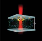
What researchers had thought of as a barrier to developing advanced technologies based on the emerging field of plasmonics is now seen as a potential pathway to practical applications in areas from cancer therapy to nanomanufacturing.
Plasmonic materials contain features, patterns or elements that enable unprecedented control of light by harnessing clouds of electrons called surface plasmons. It could allow the miniaturization of optical technologies, bringing advances such as nano-resolution imaging and computer chips that process and transmit data using light instead of electrons, representing a potential leap in performance.
However, the development of advanced optical technologies using plasmonics has been hampered because components under development cause too much light to be lost and converted into heat. But now researchers are finding that this "loss-induced plasmonic heating" could be key to development of various advanced technologies, said Vladimir M. Shalaev, co-director of the new Purdue Quantum Center, scientific director of nanophotonics at the Birck Nanotechnology Center in the university's Discovery Park and a distinguished professor of electrical and computer engineering.
The potential for practical applications using loss-induced plasmonic heating is discussed in a commentary that appeared on Jan. 22 in the Perspectives section of Science magazine. The article was written by doctoral student Justus Ndukaife, Shalaev and Alexandra Boltasseva, an associate professor of electrical and computer engineering.
"Plasmonics has generated significant interest because of the ability to squeeze light into nanoscale volumes in micro- and nano-devices, but progress has been hindered because of plasmonic losses," Ndukaife said. "We are saying we can use these losses to our advantage."
New technologies that could harness plasmonic heating include:
- A "nanotweezer" capable of positioning tiny objects quickly and accurately and freezing them in place, which could enable improved nanoscale sensing methods and aid research to manufacture advanced technologies such as quantum computers and ultra-high-resolution displays.
- A new magnetic storage technology called heat-assisted magnetic recording (HAMR), where nanoantennas, or near-field transducers, are used to focus light onto the magnetic medium. Nanoantennas could be leveraged in HAMR-based data storage. Moreover, plasmonic nanoparticles can be reshaped by heating and used to record images.
- Quadrapeutics, a clinical therapeutic approach using nanoparticles for cancer treatment. The nanoparticles are illuminated with laser light, producing plasmonic nanobubbles that can kill cancer cells.
- And a renewable energy concept that uses "plasmonic resonators" to improve the efficiency of solar cells.
"Harnessing the intrinsic loss in plasmonics could help to usher in transformative technological innovations affecting several fields, including information technology, life sciences and clean energy," Boltasseva said. "It is time for the plasmonic community to turn loss into gain."
Share on:


Testimonial
"The I-Connect007 team is outstanding—kind, responsive, and a true marketing partner. Their design team created fresh, eye-catching ads, and their editorial support polished our content to let our brand shine. Thank you all! "
Sweeney Ng - CEE PCBSuggested Items
MEMS & Imaging Sensors Summit to Spotlight Sensing Revolution for Europe’s Leadership
09/11/2025 | SEMIIndustry experts will gather November 19-20 at the SEMI MEMS & Imaging Sensors Summit 2025 to explore the latest breakthroughs in AI-driven MEMS and imaging optimization, AR/VR technologies, and advanced sensor solutions for critical defence applications.
Direct Imaging System Market Size to Hit $4.30B by 2032, Driven by Increasing Demand for High-Precision PCB Manufacturing
09/11/2025 | Globe NewswireAccording to the SNS Insider, “The Direct Imaging System Market size was valued at $2.21 Billion in 2024 and is projected to reach $4.30 Billion by 2032, growing at a CAGR of 8.68% during 2025-2032.”
I-Connect007’s Editor’s Choice: Five Must-Reads for the Week
07/04/2025 | Marcy LaRont, I-Connect007For our industry, we have seen several bullish market announcements over the past few weeks, including one this week by IDC on the massive growth in the global server market. We’re also closely watching global trade and nearshoring. One good example of successful nearshoring is Rehm Thermal Systems, which celebrates its 10th anniversary in Mexico and the official opening of its new building in Guadalajara.
Driving Innovation: Direct Imaging vs. Conventional Exposure
07/01/2025 | Simon Khesin -- Column: Driving InnovationMy first camera used Kodak film. I even experimented with developing photos in the bathroom, though I usually dropped the film off at a Kodak center and received the prints two weeks later, only to discover that some images were out of focus or poorly framed. Today, every smartphone contains a high-quality camera capable of producing stunning images instantly.
United Electronics Corporation Advances Manufacturing Capabilities with Schmoll MDI-ST Imaging Equipment
06/24/2025 | United Electronics CorporationUnited Electronics Corporation has successfully installed the advanced Schmoll MDI-ST (XL) imaging equipment at their advanced printed circuit board facility. This significant technology investment represents a continued commitment to delivering superior products and maintaining their position as an industry leader in precision PCB manufacturing.