


 Dan’s Biz Bookshelf: Four Important Books You Need to Read (Not Just Say You Have)
 The Marketing Minute: Cracking the Code of Technical Marketing


New Type of Nanowires, Built with Natural Gas Heating
February 1, 2016 | UNISTEstimated reading time: 1 minute
A team of Korean researchers, affiliated with UNIST has recently pioneered in developing a new simple nanowire manufacturing technique that uses self-catalytic growth process assisted by thermal decomposition of natural gas. According to the research team, this method is simple, reproducible, size-controllable, and cost-effective in that lithium-ion batteries could also benefit from it.
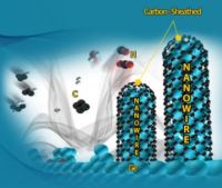
In their approach, they discovered that germanium nanowires are grown by the reduction of germanium oxide particles and subsequent self-catalytic growth during the thermal decomposition of natural gas, and simultaneously, carbon sheath layers are uniformly coated on the nanowire surface.
This study is a collaboration among scientists, including Prof. SooJin Park (School of Energy and Chemical Engineering) and Prof. Sang Kyu Kwak (School of Energy and Chemical Engineering), Dr. Sinho Choi (UNIST), Combined M.S./Ph.D. Student Dae Yeon Hwang (UNIST), and Researcher Jieun Kim (Korea Research Institute of Chemical Technology).
In a study, reported in the January 21, 2016 issue of Nano Letters, the team demonstrated a new redox-responsive assembly method to synthesize hierarchically structured carbon-sheathed germanium nanowires (c-GeNWs) on a large scale by the use of self-catalytic growth process assisted by thermally decomposed natural gas.
According to the team, this simple synthetic process not only enables them to synthesize hierachially assembled materials from inexpensive metal oxides at a larger scale, but also can likely be extended to other metal oxides as well. Moreover, the resulting hierarchically assembled nanowires (C-GeNWs) show enhanced chemical and thermal stability, as well as outstanding electrochemical properties.
The team states, "This strategy may open up an effective way to make other metallic/semiconducting nanomaterials via one-step synthetic reactions through an environmentally benign and cost-effective approach."
Share on:


Testimonial
"Advertising in PCB007 Magazine has been a great way to showcase our bare board testers to the right audience. The I-Connect007 team makes the process smooth and professional. We’re proud to be featured in such a trusted publication."
Klaus Koziol - atgSuggested Items
Alternative Manufacturing, Inc. (AMI) Announces Commitment to Excellence in Industrial, Defense, Aerospace, Renewables, and Robotics Markets
09/16/2025 | Alternative Manufacturing, Inc.Alternative Manufacturing, Inc. (AMI), a 100% employee-owned contract manufacturer, proudly reaffirms its leadership in the electronics manufacturing services (EMS) industry with a continued commitment to delivering high-quality PCBAs and box builds across the industrial, defense, aerospace, renewable energy, and robotics markets.
Sustainability and Selective Soldering
09/15/2025 | Dr. Samuel J. McMaster, Pillarhouse InternationalSustainability is more than just a buzzword for the electronics industry; it’s a key goal for all manufacturing processes. This is more than a box-ticking exercise or simply doing a small part for environmentally friendly processes. Moving toward sustainable solutions drives innovation and operational efficiency.
Trouble in Your Tank: Implementing Direct Metallization in Advanced Substrate Packaging
09/15/2025 | Michael Carano -- Column: Trouble in Your TankDirect metallization systems based on conductive graphite are gaining popularity throughout the world. The environmental and productivity gains achievable with this process are outstanding. Direct metallization reduces the costs of compliance, waste treatment, and legal issues related to chemical exposure. A graphite-based direct plate system has been devised to address these needs.
EV Group Achieves Breakthrough in Hybrid Bonding Overlay Control for Chiplet Integration
09/12/2025 | EV GroupEV Group (EVG), a leading provider of innovative process solutions and expertise serving leading-edge and future semiconductor designs and chip integration schemes, today unveiled the EVG®40 D2W—the first dedicated die-to-wafer overlay metrology platform to deliver 100 percent die overlay measurement on 300-mm wafers at high precision and speeds needed for production environments. With up to 15X higher throughput than EVG’s industry benchmark EVG®40 NT2 system designed for hybrid wafer bonding metrology, the new EVG40 D2W enables chipmakers to verify die placement accuracy and take rapid corrective action, improving process control and yield in high-volume manufacturing (HVM).
Integrating Uniplate PLBCu6 With the Digital Factory Suite
09/12/2025 | Giovanni Obino and Andreas Schatz, MKS' AtotechPrinted circuit board manufacturing is rapidly changing, driven by miniaturization, stringent reliability requirements, and growing pressure for sustainable production. Meeting these challenges requires more than incremental improvements; it demands a combination of precise equipment and real-time process intelligence. The pairing of Uniplate® PLBCu6 with the Digital Factory Suite (DFS) demonstrates how hardware and software can work together to create more responsive, resource-efficient manufacturing.