


 Dan’s Biz Bookshelf: Four Important Books You Need to Read (Not Just Say You Have)
 The Marketing Minute: Cracking the Code of Technical Marketing


Researchers Work to Annihilate Nanoscale Defects in Semiconductors
February 2, 2016 | University of ChicagoEstimated reading time: 4 minutes
Target dates are critical when the semiconductor industry adds small, enhanced features to consumer devices by integrating advanced materials onto the surfaces of computer chips. Missing a target means postponing a device’s release, which could cost a company millions of dollars or the loss of competitiveness and an entire industry.
But meeting target dates can be challenging because the final integrated devices, which include billions of transistors, must be flawless—less than one defect per 100 square centimeters.
Researchers at the University of Chicago and Argonne National Laboratory, led by Profs. Juan de Pablo and Paul Nealey, may have found a way for the semiconductor industry to hit miniaturization targets on time and without defects.
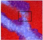
To make microchips, de Pablo and Nealey’s technique includes creating patterns on semiconductor surfaces that allow block copolymer molecules to self-assemble into specific shapes, but thinner and at much higher densities than those of the original pattern. The researchers can then use a lithography technique to create nano-trenches where conducting wire materials can be deposited.
This is a stark contrast to the industry practice of using homo-polymers in complex “photoresist” formulations, where researchers have “hit a wall,” unable to make the material smaller.
Before they could develop their new fabrication method, however, de Pablo and Nealey needed to understand exactly how block copolymers self-assemble when coated onto a patterned surface—their concern being that certain constraints cause copolymer nanostructures to assemble into undesired metastable states. To reach the level of perfection demanded to fabricate high-precision nanocircuitry, the team had to eliminate some of these metastable states.
To imagine how block copolymers assemble, it may be helpful to picture an energy landscape consisting of mountains and valleys, in which some valleys are deeper than others. The system prefers defect-free stability, which can be characterized by the deepest (low-energy) valleys, if they can be found. However, systems can get trapped inside higher (medium-energy) valleys, called metastable states, which have more defects.
To move from a metastable to stable state, block copolymer molecules must find ways to climb over the mountains and find lower energy valleys.
“Molecules in these metastable states are comfortable, and they can remain in that state for extraordinarily long periods of time,” said de Pablo.
“In order to escape such states and attain a perfect arrangement, they need to start rearranging themselves in a manner that allows the system to climb over local energy barriers, before reaching a lower energy minimum. What we have done in this work is predict the path these molecules must follow to find defect-free states and designed a process that delivers industry-standard nanocircuitry that can be scaled down to smaller densities without defects.”
Supported by a DOE leadership computing grant, de Pablo and his team used the Mira and Fusion supercomputers at the Argonne Leadership Computing Facility. The team generated molecular simulations of self-assembling block polymers along with sophisticated sampling algorithms to calculate where barriers to structural rearrangement would arise in the material.
After all the calculations were done, the researchers could precisely predict the pathways of molecular rearrangement that block copolymers must take to move from a metastable to stable state. They could also experiment with temperatures, solvents and applied fields to further manipulate and decrease the barriers between these states.
To test these calculations, de Pablo and Nealey partnered with IMEC, an international consortium located in Belgium. Their commercial-grade fabrication and characterization instruments helped the researchers perform experiments under conditions that are not available in academic laboratories. An individual defect measures only a handful of nanometers; “finding a defect in a 100-square centimeter area is like finding a needle in hay stack, and there are only a few places in the world where one has access to the necessary equipment to do so,” said de Pablo.
“Manufacturers have long been exploring the feasibility of using block copolymer assembly to reach the small critical dimensions that are demanded by modern computing and higher data storage densities,” de Pablo said. “Their biggest challenge involved evaluating defects; by following the strategies we have outlined, that challenge is greatly diminished.”
John Neuffer, president and CEO of the Semiconductor Industry Association, said industry is relentlessly focused on designing and building chips that are smaller, more powerful and more energy-efficient.
“The key to unlocking the next generation of semiconductor innovation is research,” he said. “SIA commends the work done by Argonne National Laboratory and the University of Chicago, as well as other critical scientific research being done across the United States.”
De Pablo, Nealey and their team will continue their investigations with a wider class of materials, increasing the complexity of patterns and characterizing materials in greater detail while also developing methods based on self-assembly for fabrication of three-dimensional structures.
Their long-term goal, with support from the DOE’s Office of Science, is to arrive at an understanding of directed self-assembly of polymeric molecules that will enable creation of wide classes of materials with exquisite control over their nanostructure and functionality for applications in energy harvesting, storage and transport.
Share on:


Testimonial
"In a year when every marketing dollar mattered, I chose to keep I-Connect007 in our 2025 plan. Their commitment to high-quality, insightful content aligns with Koh Young’s values and helps readers navigate a changing industry. "
Brent Fischthal - Koh YoungSuggested Items
Technica USA Advocates for PCBAA Membership Among Printed Circuit Assembly Customers
09/16/2025 | Technica USATechnica USA is actively encouraging its printed circuit assembly customers to join the Printed Circuit Board Association of America (PCBAA), a leading industry organization advocating for increased domestic production of printed circuit boards (PCBs) and substrates.
Marcy’s Musings: Advancing the Advanced Materials Discussion
09/17/2025 | Marcy LaRont -- Column: Marcy's MusingsAs the industry’s most trusted global source of original content about the electronics supply chain, we continually ask you about your concerns, what you care about, and what you most want to learn about. Your responses are insightful and valuable. Thank you for caring enough to provide useful feedback and engage in dialogue.
I-Connect007 Launches Advanced Electronics Packaging Digest
09/15/2025 | I-Connect007I-Connect007 is pleased to announce the launch of Advanced Electronics Packaging Digest (AEPD), a new monthly digital newsletter dedicated to one of the most critical and rapidly evolving areas of electronics manufacturing: advanced packaging at the interconnect level.
ICAPE Group Unveils Exclusive Report on Sustainability in Electronics Manufacturing
09/15/2025 | ICAPE GroupICAPE Group, a global leader in printed circuit boards (PCBs) and custom electronics manufacturing, today announces the launch of its 2025 Industry Outlook & Innovation Report: Sustainability in Electronics Manufacturing. This exclusive report is accompanied by fresh insights from a dedicated Statista survey of 100 electronics manufacturing professionals, commissioned by ICAPE Group.
Panasonic Industry will Double the Production Capacity of MEGTRON Multi-layer Circuit Board Materials Over the Next Five Years
09/15/2025 | Panasonic Industry Co., Ltd.Panasonic Industry Co., Ltd., a Panasonic Group company, announced plans for a major expansion of its global production capacity for MEGTRON multi-layer circuit board materials today. The company plans to double its production over the next five years to meet growing demand in the AI server and ICT infrastructure markets.