














 It’s Only Common Sense: How AI Consumes the Electronics Supply Chain
 Dan’s Biz Bookshelf: ‘Building a Story Brand 2.0’





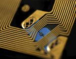
Researchers at MIT and Texas Instruments have developed a new type of radio frequency identification (RFID) chip that is virtually impossible to hack.
If such chips were widely adopted, it could mean that an identity thief couldn’t steal your credit card number or key card information by sitting next to you at a café, and high-tech burglars couldn’t swipe expensive goods from a warehouse and replace them with dummy tags.
Texas Instruments has built several prototypes of the new chip, to the researchers’ specifications, and in experiments the chips have behaved as expected. The researchers presented their research this week at the International Solid-State Circuits Conference, in San Francisco.
According to Chiraag Juvekar, a graduate student in electrical engineering at MIT and first author on the new paper, the chip is designed to prevent so-called side-channel attacks. Side-channel attacks analyze patterns of memory access or fluctuations in power usage when a device is performing a cryptographic operation, in order to extract its cryptographic key.
“The idea in a side-channel attack is that a given execution of the cryptographic algorithm only leaks a slight amount of information,” Juvekar says. “So you need to execute the cryptographic algorithm with the same secret many, many times to get enough leakage to extract a complete secret.”
One way to thwart side-channel attacks is to regularly change secret keys. In that case, the RFID chip would run a random-number generator that would spit out a new secret key after each transaction. A central server would run the same generator, and every time an RFID scanner queried the tag, it would relay the results to the server, to see if the current key was valid.
Blackout
Such a system would still, however, be vulnerable to a “power glitch” attack, in which the RFID chip’s power would be repeatedly cut right before it changed its secret key. An attacker could then run the same side-channel attack thousands of times, with the same key. Power-glitch attacks have been used to circumvent limits on the number of incorrect password entries in password-protected devices, but RFID tags are particularly vulnerable to them, since they’re charged by tag readers and have no onboard power supplies.
Two design innovations allow the MIT researchers’ chip to thwart power-glitch attacks: One is an on-chip power supply whose connection to the chip circuitry would be virtually impossible to cut, and the other is a set of “nonvolatile” memory cells that can store whatever data the chip is working on when it begins to lose power.
For both of these features, the researchers — Juvekar; Anantha Chandrakasan, who is Juvekar’s advisor and the Vannevar Bush Professor of Electrical Engineering and Computer Science; Hyung-Min Lee, who was a postdoc in Chandrakasan’s group when the work was done and is now at IBM; and TI’s Joyce Kwong, who did her master’s degree and PhD with Chandrakasan — use a special type of material known as a ferroelectric crystals.
As a crystal, a ferroelectric material consists of molecules arranged into a regular three-dimensional lattice. In every cell of the lattice, positive and negative charges naturally separate, producing electrical polarization. The application of an electric field, however, can align the cells’ polarization in either of two directions, which can represent the two possible values of a bit of information.
When the electric field is removed, the cells maintain their polarization. Texas Instruments and other chip manufacturers have been using ferroelectric materials to produce nonvolatile memory, or computer memory that retains data when it’s powered off.
Complementary capacitors
A ferroelectric crystal can also be thought of as a capacitor, an electrical component that separates charges and is characterized by the voltage between its negative and positive poles. Texas Instruments’ manufacturing process can produce ferroelectric cells with either of two voltages: 1.5 volts or 3.3 volts.
The researchers’ new chip uses a bank of 3.3-volt capacitors as an on-chip energy source. But it also features 571 1.5-volt cells that are discretely integrated into the chip’s circuitry. When the chip’s power source — the external scanner — is removed, the chip taps the 3.3-volt capacitors and completes as many operations as it can, then stores the data it’s working on in the 1.5-volt cells.
When power returns, before doing anything else the chip recharges the 3.3-volt capacitors, so that if it’s interrupted again, it will have enough power to store data. Then it resumes its previous computation. If that computation was an update of the secret key, it will complete the update before responding to a query from the scanner. Power-glitch attacks won’t work.
Because the chip has to charge capacitors and complete computations every time it powers on, it’s somewhat slower than conventional RFID chips. But in tests, the researchers found that they could get readouts from their chips at a rate of 30 per second, which should be more than fast enough for most RFID applications.
“In the age of ubiquitous connectivity, security is one of the paramount challenges we face,” says Ahmad Bahai, chief technology officer at Texas Instruments. “Because of this, Texas Instruments sponsored the authentication tag research at MIT that is being presented at ISSCC. We believe this research is an important step toward the goal of a robust, low-cost, low-power authentication protocol for the industrial Internet.”


