


 SMT Perspectives & Prospects: Artificial Intelligence Part 6: Data Module 1
 Standard of Excellence: Overcoming Service Failures—The Art of the Apology
 Nolan’s Notes: Tariffs, Technologies, and Optimization


Advance Could Aid Development of Nanoscale Biosensors
February 18, 2016 | Brown UniversityEstimated reading time: 5 minutes
Imagine a hand-held environmental sensor that can instantly test water for lead, E. coli, and pesticides all at the same time, or a biosensor that can perform a complete blood workup from just a single drop. That's the promise of nanoscale plasmonic interferometry, a technique that combines nanotechnology with plasmonics--the interaction between electrons in a metal and light.
Now researchers from Brown University's School of Engineering have made an important fundamental advance that could make such devices more practical. The research team has developed a technique that eliminates the need for highly specialized external light sources that deliver coherent light, which the technique normally requires. The advance could enable more versatile and more compact devices.
"It has always been assumed that coherent light was necessary for plasmonic interferometry," said Domenico Pacifici, a professor of engineering who oversaw the work with his postdoctoral researcher Dongfang Li, and graduate student Jing Feng. "But we were able to disprove that assumption."
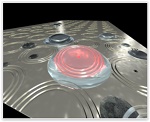
Plasmonic interferometers make use of the interaction between light and surface plasmon polaritons, density waves created when light energy rattles free electrons in a metal. One type of interferometer looks like a bull's-eye structure etched into a thin layer of metal. In the center is a hole poked through the metal layer with a diameter of about 300 nanometers--about 1,000 times smaller than the diameter of a human hair. The hole is encircled by a series of etched grooves, with diameters of a few micrometers. Thousands of these bulls-eyes can be placed on a chip the size of a fingernail.
When light from an external source is shown onto the surface of an interferometer, some of the photons go through the central hole, while others are scattered by the grooves. Those scattered photons generate surface plasmons that propagate through the metal inward toward the hole, where they interact with photons passing through the hole. That creates an interference pattern in the light emitted from the hole, which can be recorded by a detector beneath the metal surface.
When a liquid is deposited on top of an interferometer, the light and the surface plasmons propagate through that liquid before they interfere with each other. That alters the interference patterns picked up by the detector depending on the chemical makeup of the liquid or compounds present in it. By using different sizes of groove rings around the hole, the interferometers can be tuned to detect the signature of specific compounds or molecules. With the ability to put many differently tuned interferometers on one chip, engineers can hypothetically make a versatile detector.
Up to now, all plasmonic interferometers have required the use of highly specialized external light sources that can deliver coherent light--beams in which light waves are parallel, have the same wavelength, and travel in-phase (meaning the peaks and valleys of the waves are aligned). Without coherent light sources, the interferometers cannot produce usable interference patterns. Those kinds of light sources, however, tend to be bulky, expensive, and require careful alignment and periodic recalibration to obtain a reliable optical response.
But Pacifici and his group have come up with a way to eliminate the need for external coherent light. In the new method, fluorescent light-emitting atoms are integrated directly within the tiny hole in the center of the interferometer. An external light source is still necessary to excite the internal emitters, but it need not be a specialized coherent source.
"This is a whole new concept for optical interferometry," Pacifici said, "an entirely new device."
In this new device, incoherent light shown on the interferometer causes the fluorescent atoms inside the center hole to generate surface plasmons. Those plasmons propagate outward from the hole, bounce off the groove rings, and propagate back toward the hole after. Once a plasmon propagates back, it interacts with the atom that released it, causing an interference with the directly transmitted photon. Because the emission of a photon and the generation of a plasmon are indistinguishable, alternative paths originating from the same emitter, the process is naturally coherent and interference can therefore occur even though the emitters are excited incoherently.
"The important thing here is that this is a self-interference process," Pacifici said. "It doesn't matter that you're using incoherent light to excite the emitters, you still get a coherent process."
In addition to eliminating the need for specialized external light sources, the approach has several advantages, Pacifici said. Because the surface plasmons travel out from the hole and back again, they probe the sample on top of the interferometer surface twice. That makes the device more sensitive.
But that's not the only advantage. In the new device, external light can be projected from underneath the metal surface containing the interferometers instead of from above. That eliminates the need for complex illumination architectures on top of the sensing surface, which could make for easier integration into compact devices.
The embedded light emitters also eliminate the need to control the amount of sample liquid deposited on the interferometer's surface. Large droplets of liquid can cause lensing effects, a bending of light that can scramble the results from the interferometer. Most plasmonic sensors make use of tiny microfluidic channels to deliver a thin film of liquid to avoid lensing problems. But with internal light emitters excited from the bottom surface, the external light never comes in contact with the sample, so lensing effects are negated, as is the need for microfluidics.
Finally, the internal emitters produce a low intensity light. That's good for probing delicate samples, such as proteins, than can be damaged by high-intensity light.
More work is required to get the system out of the lab and into devices, and Pacifici and his team plan to continue to refine the idea. The next step will be to try eliminating the external light source altogether. It might be possible, the researchers say, to eventually excite the internal emitters using tiny fiber optic lines, or perhaps electric current.
Still, this initial proof-of-concept is promising, Pacifici said.
"From a fundamental standpoint, we think this new device represents a significant step forward," he said, "a first demonstration of plasmonic interferometry with incoherent light".
Share on:


Testimonial
"We’re proud to call I-Connect007 a trusted partner. Their innovative approach and industry insight made our podcast collaboration a success by connecting us with the right audience and delivering real results."
Julia McCaffrey - NCAB GroupSuggested Items
Beyond Thermal Conductivity: Exploring Polymer-based TIM Strategies for High-power-density Electronics
10/13/2025 | Padmanabha Shakthivelu and Nico Bruijnis, MacDermid Alpha Electronics SolutionsAs power density and thermal loads continue to increase, effective thermal management becomes increasingly important. Rapid and efficient heat transfer from power semiconductor chip packages is essential for achieving optimal performance and ensuring long-term reliability of temperature-sensitive components. This is particularly crucial in power systems that support advanced applications such as green energy generation, electric vehicles, aerospace, and defense, along with high-speed computing for data centers and artificial intelligence (AI).
Driving Innovation: Depth Routing Processes—Achieving Unparalleled Precision in Complex PCBs
09/08/2025 | Kurt Palmer -- Column: Driving InnovationIn PCB manufacturing, the demand for increasingly complex and miniaturized designs continually pushes the boundaries of traditional fabrication methods, including depth routing. Success in these applications demands not only on robust machinery but also sophisticated control functions. PCB manufacturers rely on advanced machine features and process methodologies to meet their precise depth routing goals. Here, I’ll explore some crucial functions that empower manufacturers to master complex depth routing challenges.
Polar Instruments Announces Additive Transmission Line Support for Si9000e
08/20/2025 | Polar InstrumentsTransmission lines embedded into the PCB surface are a feature of UHDI constructions. The 2025 fall release of Polar's Si9000e PCB impedance & insertion loss transmission line field solver incorporates eight new single ended, differential and coplanar transmission line structures.
Henniker Plasma Launches Stratus Turnkey Plasma Manufacturing Cell
08/13/2025 | Henniker PlasmaHenniker Plasma, a leading manufacturer of plasma treatment systems, proudly announces the launch of its Stratus Plasma Manufacturing Cell range — a fully integrated, turnkey solution that combines advanced atmospheric plasma surface treatment with robotic automation.
Trouble in Your Tank: Metallizing Flexible Circuit Materials—Mitigating Deposit Stress
08/04/2025 | Michael Carano -- Column: Trouble in Your TankMetallizing materials, such as polyimide used for flexible circuitry and high-reliability multilayer printed wiring boards, provide a significant challenge for process engineers. Conventional electroless copper systems often require pre-treatments with hazardous chemicals or have a small process window to achieve uniform coverage without blistering. It all boils down to enhancing the adhesion of the thin film of electroless copper to these smooth surfaces.