


 Fresh PCB Concepts: Engineering Copper Coin and Copper Pedestal Technology With IPC Design Interpretation
 Target Condition: Signal Integrity Without Borders
 Elementary, Mr. Watson: PCB Education in the Midst of the Storms


Ventec International Group, a world leader in the production of polyimide and high-reliability epoxy laminates and prepregs, unveiled their high-speed/low-loss product portfolio, tec-speed, in January 2016. Ventec will be showcasing the range globally at a number of shows this year. Starting with IPC APEX EXPO in Las Vegas (15-17 March 2016), tec-speed will be a highlight at Ventec’s booth number 827 with an emphasis on the mil/aero applications.
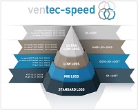
Tec-speed unites Ventec's high-speed/low-loss product portfolio and better positions the range under a single identity, connecting the products through a clear and cohesive visual presentation. The tec-speed laminates and prepregs range from mid-loss (Df 0.012) to ultra-low-loss (Df 0.003) specifications with Dk levels ranging between 3.9 and 3.2, offering the ultimate in laminate technology and quality assurance through Ventec's proprietary manufacturing and distribution network.
Jack Pattie, president of Ventec USA, said, “Thermal performance and signal integrity demands are increasing, particularly for mil/aero applications where miniaturization and density of components are pushing the boundaries of PCB design. Tec-speed materials and our strategic roadmap of new innovative additions to the range, provide the technological innovation, high performance and quality demanded by our customers.”
A selection of products will be highlighted at the show, including:
- tec-speed 6.1 (Dk 3.2, Df 0.004 RC 50%) - Ultra-Low Loss High-Tg material available with all copper styles, including HVLP. Uses low Dk spread glass to improve skew and jitter. Applications include telecom, router, servers, etc. Specifically developed for backplane and daughter card designs where good signal integrity is essential. This material has excellent thermal properties.
- tec-speed 4.0 (Dk 3.8, Df 0.007) - Low-loss high-Tg material available with all copper styles, including HVLP. Applications focus on high-frequency and high-speed designs, Automotive and satellite communication, Navigation and GPS are typical applications. This material has excellent thermal properties.
- tec-speed 1.0 (Dk 3.9, Df 0.012 @ 10GHz RC75%) - Mid-loss mid-Tg halogen-free material available with all copper styles. Applications include hand-held products, specifically those that require high-frequency high-speed materials. This material has excellent thermal properties.
About Ventec International
With volume manufacturing facilities and HQ in Suzhou China, Ventec International specializes in advanced copper clad glass reinforced and metal backed substrates for the PCB industry. With distribution locations and quick-turn CCL manufacturing sites in both the US and Europe, Ventec International is a premier supplier to the Global PCB industry. For more information about Ventec’s solutions and the company’s wide variety of products, please click here or download to the Ventec APP.


