


 Dan’s Biz Bookshelf: Four Important Books You Need to Read (Not Just Say You Have)
 The Marketing Minute: Cracking the Code of Technical Marketing


Irregular Silicon Wafer Breakage Studied in Real-time
March 4, 2016 | International Union of CrystallographyEstimated reading time: 1 minute
Fracture and breakage of single crystals, particularly of silicon wafers, are multi-scale problems: the crack tip starts propagating on an atomic scale with the breaking of chemical bonds, forms crack fronts through the crystal on the micrometre scale and ends macroscopically in catastrophic wafer shattering.
Total wafer breakage is a severe problem for the semiconductor industry not only during handling but also during temperature treatments, leading to million-dollar costs per annum in a device production line. Knowledge of the relevant dynamics governing perfect cleavage along the {111} or {110} faces, and of the deflection into higher indexed {hkl} faces of higher energy, is scarce due to the high velocity of the process. Imaging techniques are commonly limited to depicting only the state of a wafer before the crack and in the final state.
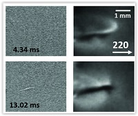
A group of researchers demonstrates, for the first time, in situ high-speed crack propagation under thermal stress, imaged simultaneously in direct transmission and diffraction X-ray imaging. A scientific commentary also exists. The scientists show how the propagating crack tip and the related strain field can be tracked in the phase-contrast and diffracted images, respectively. Movies with a time resolution of microseconds per frame reveal that the strain and crack tip do not propagate continuously or at a constant speed. Jumps in the crack tip position indicate pinning of the crack tip for about 1-2 ms followed by jumps faster than 2-6 m s-1, leading to a macroscopically observed average velocity of 0.028-0.055 m s-1. The results also give a proof of concept that the described X-ray technique is compatible with studying ultra-fast cracks up to the speed of sound.
Rack et al. comment, “We are only at the beginning of studying ultra-fast crack propagation in single-crystalline materials in real time”.
Share on:


Testimonial
"We’re proud to call I-Connect007 a trusted partner. Their innovative approach and industry insight made our podcast collaboration a success by connecting us with the right audience and delivering real results."
Julia McCaffrey - NCAB GroupSuggested Items
TRI to Unveil New High-Throughput AOI and AXI at productronica 2023
09/15/2023 | TRITest Research, Inc. (TRI), the leading test and inspection systems provider for the electronics manufacturing industry, will join productronica 2023, which will be held at Messe München Center from November 14 – 17, 2023.
UK Space Agency Launches Consultation on Variable Liability Limits for Orbital Operations
09/15/2023 | UK Space AgencyThe proposals from the UK Space Agency follow a review into the UK’s approach to setting the amount of an operator’s liability in licences for orbital operations, a key commitment of the government’s National Space Strategy.
MediaTek Successfully Develops First Chip Using TSMC's 3nm Process, Set for Volume Production in 2024
09/14/2023 | MediaTekMediaTek and TSMC announced that MediaTek has successfully developed its first chip using TSMC's leading-edge 3nm technology, taping out MediaTek’s flagship Dimensity system-on-chip (SoC) with volume production expected next year.
MKS’ Atotech to Participate in IPCA Expo 2023
09/14/2023 | MKS’ AtotechMKS’ Atotech, a leading surface finishing brand of MKS Instruments, will participate in the upcoming IPCA Expo at Bangalore International Exhibition Centre (BIEC) and showcase its latest PCB manufacturing solutions from September 13 – 15.
Comtech Unveils New BRIDGE Solutions to Increase Access to Global Hybrid Connectivity
09/12/2023 | Business WireComtech launched its new blended, resilient, integrated, digital, global, end-to-end (BRIDGE) connectivity solutions. Comtech’s BRIDGE solutions provide portable, adaptable, full-service communications networks that can be established in a matter of hours and help “bridge the gap” for traditional satellite and terrestrial infrastructures.