


 Dan’s Biz Bookshelf: Four Important Books You Need to Read (Not Just Say You Have)
 The Marketing Minute: Cracking the Code of Technical Marketing


Overlooked Resistance May Inflate Estimates of Organic-Semiconductor Performance
March 10, 2016 | NISTEstimated reading time: 3 minutes
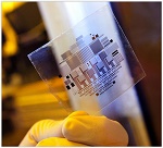
It's hardly a character flaw, but organic transistors--the kind envisioned for a host of flexible electronics devices--behave less than ideally, or at least not up to the standards set by their rigid, predictable silicon counterparts. When unrecognized, a new study finds, this disparity can lead to gross overestimates of charge-carrier mobility, a property key to the performance of electronic devices.
If measurements fail to account for these divergent behaviors in so-called "organic field-effect transistors" (OFETs), the resulting estimates of how fast electrons or other charge carriers travel in the devices may be more than 10 times too high, report researchers from the National Institute of Standards and Technology (NIST), Wake Forest University and Penn State University. The team's measurements implicate an overlooked source of electrical resistance as the root of inaccuracies that can inflate estimates of organic semiconductor performance.
Already used in light-emitting diodes, or LEDs, electrically conductive polymers and small molecules are being groomed for applications in flexible displays, flat-panel TVs, sensors, "smart" textiles, solar cells and "Internet of Things" applications. Besides flexibility, a key selling point is that the organic devices--sometimes called "plastic electronics"--can be manufactured in large volumes and far more inexpensively than today's ubiquitous silicon-based devices.
A key sticking point, however, is the challenge of achieving the high levels of charge-carrier mobility that these applications require. In the semiconductor arena, the general rule is that higher mobility is always better, enabling faster, more responsive devices. So chemists have set out to hurry electrons along. Working from a large palette of organic materials, they have been searching for chemicals--alone or in combination--that will up the speed limit in their experimental devices.
Just as for silicon semiconductors, assessments of performance require measurements of current and voltage. In the basic transistor design, a source electrode injects charge into the transistor channel leading to a drain electrode. In between sits a gate electrode that regulates the current in the channel by applying voltage, functioning much like a valve.
Typically, measurements are analyzed according to a longstanding theory for silicon field-effect transistors. Plug in the current and voltage values and the theory can be used to predict properties that determine how well the transistor will perform in a circuit.
Results are rendered as a series of "transfer curves." Of particular interest in the new study are curves showing how the drain current changes in response to a change in the gate electrode voltage. For devices with ideal behavior, this relationship provides a good measure of how fast charge carriers move through the channel to the drain.
"Organic semiconductors are more prone to non-ideal behavior because the relatively weak intermolecular interactions that make them attractive for low-temperature processing also limit the ability to engineer efficient contacts as one would for state-of-the-art silicon devices," says electrical engineer David Gundlach, who leads NIST's Thin Film Electronics Project. "Since there are so many different organic materials under investigation for electronics applications, we decided to step back and do a measurement check on the conventional wisdom."
Using what Gundlach describes as the semiconductor industry's "workhorse" measurement methods, the team scrutinized an OFET made of single-crystal rubrene, an organic semiconductor with a molecule shaped a bit like a microscale insect. Their measurements revealed that electrical resistance at the source electrode--the contact point where current is injected into the OFET-- significantly influences the subsequent flow of electrons in the transistor channel, and hence the mobility.
In effect, contact resistance at the source electrode creates the equivalent of a second valve that controls the entry of current into the transistor channel. Unaccounted for in the standard theory, this valve can overwhelm the gate--the de facto¬ regulator between the source and drain in a silicon semiconductor transistor--and become the dominant influence on transistor behavior.
At low gate voltages, this contact resistance at the source can overwhelm device operation. Consequently, model-based estimates of charge-carrier mobility in organic semiconductors may be more than 10 times higher than the actual value, the research team reports.
Hardly ideal behavior, but the aim of the study, the researchers write, is to improve "understanding of the source of the non-ideal behavior and its impact on extracted figures of merit," especially charge-carrier mobility. This knowledge, they add, can inform efforts to develop accurate, comprehensive measurement methods for benchmarking organic semiconductor performance, as well as guide efforts to optimize contact interfaces.
Share on:


Testimonial
"The I-Connect007 team is outstanding—kind, responsive, and a true marketing partner. Their design team created fresh, eye-catching ads, and their editorial support polished our content to let our brand shine. Thank you all! "
Sweeney Ng - CEE PCBSuggested Items
iDEAL Semiconductor Announces Polar Semiconductor as Manufacturing Partner for SuperQ™ Power Devices
09/18/2025 | PRNewswireiDEAL Semiconductor confirms that its ultra-efficient SuperQ™ silicon power devices are now in production at Polar Semiconductor, a leading foundry specializing in high-voltage, power, and sensor technologies.
Global Interposer Market to Surge Nearly Fivefold by 2034
09/15/2025 | I-Connect007 Editorial TeamRevenue for the global interposer market is projected to climb from $471 million in 2025 to more than $2.3 billion by 2034, according to a new report from Business Research Insights. The growth represents a CAGR of nearly 20 percent over the forecast period.
Zhen Ding Drives AI-Powered Digital Transformation
09/12/2025 | Zhen DingDriven by the surging demand for computing power fueled by AI, the semiconductor and PCB industries are forging closer integration, expanding their ecosystems, and pursuing shared growth. PCB has already become another NT$ trillion-dollar industry in Taiwan, growing in tandem with the semiconductor sector.
Zhen Ding Expands PCB into Semiconductors at SEMICON Taiwan 2025; Advantech Drives AI Smart Parks
09/12/2025 | Zhen DingZhen Ding Technology Holding Co., Ltd., a global leader in the PCB industry, returned to exhibit at SEMICON Taiwan 2025. Positioning itself as an industry pioneer in "PCB expanding into semiconductors," the company showcased its latest strategic layout
SkyWater Completes Acquisition of Fab 25, Expanding U.S. Pure-Play Foundry Capacity for Critical Semiconductor Technologies
09/12/2025 | SkyWaterSkyWater Technology, the trusted technology realization partner, announced that it has completed its acquisition of Infineon Technologies AG’s 200 mm semiconductor fab in Austin, Texas (“Fab 25”)