


 Dan’s Biz Bookshelf: ‘Elevate: Push Beyond Your Limits'
 The Marketing Minute: The First Step to More Sales—Marketing
 It’s Only Common Sense: Customer Service Is Sales in Disguise


New LPKF Contac S4 for Galvanic Through-hole Plating
March 15, 2016 | LPKFEstimated reading time: 2 minutes
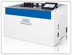
In the manufacturing of double-sided or multilayer PCBs, reliable electrical connection of the conductive networks is essential. At Embedded World in February 2016, LPKF will present the compact Contac S4 system for galvanic through-hole plating without the need for any knowledge of chemistry.
Complex electronic circuits have outgrown single-sided boards. The backs of the boards must also transmit current or signals; in addition, as complexity increases, the number of layers required also increases. Currently prototypes with up to eight layers can be produced in the lab. Various methods are available for connecting the layers.
Copper rivets can be used in a few cases for through holes with relatively large hole diameters. Copper rivets and punch tools with various diameters are available.
Another method uses a specially designed paste that is pulled through the holes by a vacuum and then cured in a furnace. Holes with diameters of up to 0.4 mm can be contacted reliably with a resistance of 20 mΩ.
The LPKF Contac S4 can be used for reliable, homogeneous through-hole plating of up to eight layers in the lab.
For assembly production prototypes, multilayers, and small holes with diameters of up to 0.2 mm, galvanic through-hole plating is the best option. In this process, holes are introduced into the unstructured base material, which is then given a conductive coating. The boards are electrically contacted and suspended in a galvanic bath. Copper is built up on every conductive surface in a galvanic process. The LPKF Contac S4 has six baths for performing all the necessary steps: activation, cleaning, and galvanization. In addition, tin plating can be performed in one of the baths to provide surface protection and improve solderability.
The LPKF Contac S4 underwent a number of changes from the predecessor models: A new anode plate design in conjunction with reverse pulse plating ensures highly homogeneous copper layer buildup with a layer tolerance of a mere ± 2 µm. Boards contacted in this way can be structured easily, e.g., with the LPKF ProtoLaser S4 (laser source in the green range of the visible light spectrum) without any damage being done to the organic substrate. A cleaning step for microvias also guarantees the quality of the contacts, even with fine holes with an aspect ratio of 1:10.
A new operating concept with a touch panel is being used for the first time in the LPKF Contac S4. The wizard guides the user through each step of the process and ensures that the process can be performed by any user, with or without any knowledge of chemistry.
The system requires very little maintenance and is made of high-quality discoloration-resistant materials.
About LPKF
Established in 1976, LPKF Laser & Electronics manufactures milling machines and laser systems used in circuit board and microelectronics fabrication, medical technology, the automotive sector, and the production of solar cells. LPKF’s worldwide headquarters is located in Hannover, Germany and its North American headquarters resides near Portland, Ore.
Share on:


Suggested Items
I-Connect007 Editor’s Choice: Five Must-Reads for the Week
07/18/2025 | Nolan Johnson, I-Connect007It may be the middle of the summer, but the news doesn’t quit, and there’s plenty to talk about this week, whether you’re talking technical or on a global scale. When I have to choose six items instead of my regular five, you know it’s good. I start by highlighting my interview with Martyn Gaudion on his latest book, share some concerning tariff news, follow that up with some promising (and not-so-promising) investments, and feature a paper from last January’s inaugural Pan-European Design Conference.
Elephantech Launches World’s Smallest-Class Copper Nanofiller
07/17/2025 | ElephantechJapanese deep-tech startup Elephantech has launched its cutting-edge 15 nm class copper nanofiller – the smallest class available globally. This breakthrough makes Elephantech one of the first companies in the world to provide such advanced material for commercial use.
Copper Price Surge Raises Alarms for Electronics
07/15/2025 | Global Electronics Association Advocacy and Government Relations TeamThe copper market is experiencing major turbulence in the wake of U.S. President Donald Trump’s announcement of a 50% tariff on imported copper effective Aug. 1. Recent news reports, including from the New York Times, sent U.S. copper futures soaring to record highs, climbing nearly 13% in a single day as manufacturers braced for supply shocks and surging costs.
I-Connect007 Editor’s Choice: Five Must-Reads for the Week
07/11/2025 | Andy Shaughnessy, Design007 MagazineThis week, we have quite a variety of news items and articles for you. News continues to stream out of Washington, D.C., with tariffs rearing their controversial head again. Because these tariffs are targeted at overseas copper manufacturers, this news has a direct effect on our industry.I-Connect007 Editor’s Choice: Five Must-Reads for the Week
Digital Twin Concept in Copper Electroplating Process Performance
07/11/2025 | Aga Franczak, Robrecht Belis, Elsyca N.V.PCB manufacturing involves transforming a design into a physical board while meeting specific requirements. Understanding these design specifications is crucial, as they directly impact the PCB's fabrication process, performance, and yield rate. One key design specification is copper thieving—the addition of “dummy” pads across the surface that are plated along with the features designed on the outer layers. The purpose of the process is to provide a uniform distribution of copper across the outer layers to make the plating current density and plating in the holes more uniform.