


 Dan’s Biz Bookshelf: Four Important Books You Need to Read (Not Just Say You Have)
 The Marketing Minute: Cracking the Code of Technical Marketing


New ORNL Method Could Unleash Solar Power Potential
March 16, 2016 | ORNLEstimated reading time: 2 minutes
Measurement and data analysis techniques developed at the Department of Energy's Oak Ridge National Laboratory could provide new insight into performance-robbing flaws in crystalline structures, ultimately improving the performance of solar cells.
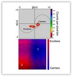
While solar cells made from light-harvesting perovskite (an organic-inorganic hybrid) materials have recently eclipsed the 20 percent efficiency mark, researchers believe they could do better if they had a clearer picture of energy flow at the nanometer scale. The ORNL discovery, described in a paper published in ACS Photonics, synchronizes microscopy, ultra-short pulses of laser light and data analytics to extract images with single-pixel precision, providing unprecedented detail.
"If we can see exactly and in real time what is happening, we can map out the electronic processes in space instead of relying on snapshots gleaned from spatial averages," said Benjamin Doughty, one of the authors and a member of ORNL's Chemical Sciences Division.
Armed with information about what electrons are doing inside the material, researchers believe they can make improvements that lead to solar cells that are more efficient and potentially less expensive.
"With conventional approaches of studying photovoltaic materials, we are unable to accurately map out electronic processes and how electrons are getting lost," Doughty said. "Those processes can translate into losses in efficiency."
The experiment consists of optically pumping the thin film sample with a 50 femtosecond -- or 50 millionths of a billionth of a second -- laser pulse and then measuring changes in light absorption with a second laser pulse in the material. The technique, called femtosecond transient absorption microscopy, consists of a tabletop of lasers, optics and a microscope. The net result is a pixel-by-pixel map of the material being studied and information researchers can use to improve performance.
"The ability to identify what will be created after the solar cell absorbs a photon, either a pair of free charges or their bound form called an exciton, is crucial from both fundamental and applied perspectives," said co-author Yingzhong Ma, who led the research team. "We found that both free charges and excitons are present, and the strength of our approach lies in not only identifying where they are but also determining what their relative contributions are when they are both present at a given spatial location."
A key remaining challenge is to understand what causes the observed spatial difference, said Ma, so he and colleagues are exploring an all-optical imaging approach that would allow them to correlate electronic dynamics with underlying structural information. This approach may also help researchers map and understand perovskite degradation issues associated with moisture. Ma noted that this must be resolved before solar cells based on this class of materials can be successful.
Share on:


Testimonial
"In a year when every marketing dollar mattered, I chose to keep I-Connect007 in our 2025 plan. Their commitment to high-quality, insightful content aligns with Koh Young’s values and helps readers navigate a changing industry. "
Brent Fischthal - Koh YoungSuggested Items
Curing and Verification in PCB Shadow Areas
09/17/2025 | Doug Katze, DymaxDesign engineers know a simple truth that often complicates electronics manufacturing: Light doesn’t go around corners. In densely populated PCBs, adhesives and coatings often fail to fully cure in shadowed regions created by tall ICs, connectors, relays, and tight housings.
Marcy’s Musings: Advancing the Advanced Materials Discussion
09/17/2025 | Marcy LaRont -- Column: Marcy's MusingsAs the industry’s most trusted global source of original content about the electronics supply chain, we continually ask you about your concerns, what you care about, and what you most want to learn about. Your responses are insightful and valuable. Thank you for caring enough to provide useful feedback and engage in dialogue.
September 2025 PCB007 Magazine: The Future of Advanced Materials
09/16/2025 | I-Connect007 Editorial TeamMoore’s Law is no more, and the advanced material solutions being developed to grapple with this reality are surprising, stunning, and perhaps a bit daunting. Buckle up for a dive into advanced materials and a glimpse into the next chapters of electronics manufacturing.
I-Connect007 Launches Advanced Electronics Packaging Digest
09/15/2025 | I-Connect007I-Connect007 is pleased to announce the launch of Advanced Electronics Packaging Digest (AEPD), a new monthly digital newsletter dedicated to one of the most critical and rapidly evolving areas of electronics manufacturing: advanced packaging at the interconnect level.
Panasonic Industry will Double the Production Capacity of MEGTRON Multi-layer Circuit Board Materials Over the Next Five Years
09/15/2025 | Panasonic Industry Co., Ltd.Panasonic Industry Co., Ltd., a Panasonic Group company, announced plans for a major expansion of its global production capacity for MEGTRON multi-layer circuit board materials today. The company plans to double its production over the next five years to meet growing demand in the AI server and ICT infrastructure markets.