


 Dan’s Biz Bookshelf: Four Important Books You Need to Read (Not Just Say You Have)
 The Marketing Minute: Cracking the Code of Technical Marketing


Printing Nanomaterials with Plasma
March 23, 2016 | AIP.orgEstimated reading time: 2 minutes
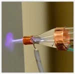
Printing has come a long way since the days of Johannes Gutenberg. Now, researchers have developed a new method that uses plasma to print nanomaterials onto a 3-D object or flexible surface, such as paper or cloth. The technique could make it easier and cheaper to build devices like wearable chemical and biological sensors, flexible memory devices and batteries, and integrated circuits.
One of the most common methods to deposit nanomaterials--such as a layer of nanoparticles or nanotubes--onto a surface is with an inkjet printer similar to an ordinary printer found in an office. Although they use well-established technology and are relatively cheap, inkjet printers have limitations. They can't print on textiles or other flexible materials, let alone 3-D objects. They also must print liquid ink, and not all materials are easily made into a liquid.
Some nanomaterials can be printed using aerosol printing techniques. But the material must be heated several hundreds of degrees to consolidate into a thin and smooth film. The extra step is impossible for printing on cloth or other materials that can burn, and means higher cost for the materials that can take the heat.
The plasma method skips this heating step and works at temperatures not much warmer than 40 degrees Celsius. "You can use it to deposit things on paper, plastic, cotton, or any kind of textile," said Meyya Meyyappan of NASA Ames Research Center. "It's ideal for soft substrates." It also doesn't require the printing material to be liquid.
The researchers, from NASA Ames and SLAC National Accelerator Laboratory, describe their work in Applied Physics Letters, from AIP Publishing>.
They demonstrated their technique by printing a layer of carbon nanotubes on paper. They mixed the nanotubes into a plasma of helium ions, which they then blasted through a nozzle and onto paper. The plasma focuses the nanoparticles onto the paper surface, forming a consolidated layer without any need for additional heating.
The team printed two simple chemical and biological sensors. The presence of certain molecules can change the electrical resistance of the carbon nanotubes. By measuring this change, the device can identify and determine the concentration of the molecule. The researchers made a chemical sensor that detects ammonia gas and a biological sensor that detects dopamine, a molecule linked to disorders like Parkinson's disease and epilepsy.
But these were just simple proofs-of-principle, Meyyappan said. "There's a wide range of biosensing applications." For example, you can make sensors that monitor health biomarkers like cholesterol, or food-borne pathogens like E. coli and Salmonella.
Because the method uses a simple nozzle, it's versatile and can be easily scaled up. For example, a system could have many nozzles like a showerhead, allowing it to print on large areas. Or, the nozzle could act like a hose, free to spray nanomaterials on the surfaces of 3-D objects.
"It can do things inkjet printing cannot do," Meyyappan said. "But anything inkjet printing can do, it can be pretty competitive."
The method is ready for commercialization, Meyyappan said, and should be relatively inexpensive and straightforward to develop. Right now, the researchers are designing the technique to print other kinds of materials such as copper. They can then print materials used for batteries onto thin sheets of metal such as aluminum. The sheet can then be rolled into tiny batteries for cellphones or other devices.
Share on:


Testimonial
"Our marketing partnership with I-Connect007 is already delivering. Just a day after our press release went live, we received a direct inquiry about our updated products!"
Rachael Temple - AlltematedSuggested Items
Electrodeposited Copper Foils Market to Grow by $11.7 Billion Over 2025-2032
09/18/2025 | Globe NewswireThe global electrodeposited copper foils market is poised for dynamic growth, driven by the rising adoption in advanced electronics and renewable energy storage solutions.
MacDermid Alpha Showcases Advanced Interconnect Solutions at PCIM Asia 2025
09/18/2025 | MacDermid Alpha Electronics SolutionsMacDermid Alpha Electronic Solutions, a global leader in materials for power electronics and semiconductor assembly, will showcase its latest interconnect innovations in electronic interconnect materials at PCIM Asia 2025, held from September 24 to 26 at the Shanghai New International Expo Centre, Booth N5-E30
Trouble in Your Tank: Implementing Direct Metallization in Advanced Substrate Packaging
09/15/2025 | Michael Carano -- Column: Trouble in Your TankDirect metallization systems based on conductive graphite are gaining popularity throughout the world. The environmental and productivity gains achievable with this process are outstanding. Direct metallization reduces the costs of compliance, waste treatment, and legal issues related to chemical exposure. A graphite-based direct plate system has been devised to address these needs.
Closing the Loop on PCB Etching Waste
09/09/2025 | Shawn Stone, IECAs the PCB industry continues its push toward greener, more cost-efficient operations, Sigma Engineering’s Mecer System offers a comprehensive solution to two of the industry’s most persistent pain points: etchant consumption and rinse water waste. Designed as a modular, fully automated platform, the Mecer System regenerates spent copper etchants—both alkaline and acidic—and simultaneously recycles rinse water, transforming a traditionally linear chemical process into a closed-loop system.
Driving Innovation: Depth Routing Processes—Achieving Unparalleled Precision in Complex PCBs
09/08/2025 | Kurt Palmer -- Column: Driving InnovationIn PCB manufacturing, the demand for increasingly complex and miniaturized designs continually pushes the boundaries of traditional fabrication methods, including depth routing. Success in these applications demands not only on robust machinery but also sophisticated control functions. PCB manufacturers rely on advanced machine features and process methodologies to meet their precise depth routing goals. Here, I’ll explore some crucial functions that empower manufacturers to master complex depth routing challenges.