















 It’s Only Common Sense: How AI Consumes the Electronics Supply Chain
 Dan’s Biz Bookshelf: ‘Building a Story Brand 2.0’





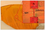
The transistor is the most fundamental building block of electronics, used to build circuits capable of amplifying electrical signals or switching them between the 0s and 1s at the heart of digital computation. Transistor fabrication is a highly complex process, however, requiring high-temperature, high-vacuum equipment.
Now, University of Pennsylvania engineers have shown a new approach for making these devices: sequentially depositing their components in the form of liquid nanocrystal “inks.”
Their new study, published in Science, opens the door for electrical components to be built into flexible or wearable applications, as the lower-temperature process is compatible with a wide array of materials and can be applied to larger areas.
The researchers’ nanocrystal-based field effect transistors were patterned onto flexible plastic backings using spin coating but could eventually be constructed by additive manufacturing systems, like 3-D printers.
The study was lead by Cherie Kagan, the Stephen J. Angello Professor in the School of Engineering and Applied Science, and Ji-Hyuk Choi, then a member of her lab, now a senior researcher at the Korea Institute of Geoscience and Mineral Resources. Han Wang, Soong Ju Oh, Taejong Paik and Pil Sung Jo of the Kagan lab contributed to the work. They collaborated with Christopher Murray, a Penn Integrates Knowledge Professor with appointments in the School of Arts & Sciences and Penn Engineering; Murray lab members Xingchen Ye and Benjamin Diroll; and Jinwoo Sung of Korea’s Yonsei University.
The researchers began by taking nanocrystals, or roughly spherical nanoscale particles, with the electrical qualities necessary for a transistor and dispersing these particles in a liquid, making nanocrystal inks.
Kagan’s group developed a library of four of these inks: a conductor (silver), an insulator (aluminum oxide), a semiconductor (cadmium selenide) and a conductor combined with a dopant (a mixture of silver and indium). “Doping” the semiconductor layer of the transistor with impurities controls whether the device transmits a positive or negative charge.
“These materials are colloids just like the ink in your inkjet printer,” Kagan said, “but you can get all the characteristics that you want and expect from the analogous bulk materials, such as whether they’re conductors, semiconductors or insulators.
“Our question was whether you could lay them down on a surface in such a way that they work together to form functional transistors.”
The electrical properties of several of these nanocrystal inks had been independently verified, but they had never been combined into full devices.
“This is the first work,” Choi said, “showing that all the components, the metallic, insulating, and semiconducting layers of the transistors, and even the doping of the semiconductor could be made from nanocrystals.”
Such a process entails layering or mixing them in precise patterns.
Page 1 of 2
Share on:



Subscribe
Stay ahead of the technologies shaping the future of electronics with our latest newsletter, Advanced Electronics Packaging Digest. Get expert insights on advanced packaging, materials, and system-level innovation, delivered straight to your inbox.
Subscribe now to stay informed, competitive, and connected.
Suggested Items
I-Connect007 Editor’s Choice: Five Must-Reads for the Week
09/25/2026 | Michelle Te, I-Connect007I recently discovered that the original “Star Trek” debuted in the same month I was born. You can look that up if you want to, but did you know that the series only ran for three years? During that time, however, they produced nearly 30 episodes per season, so there were more than 80 episodes to run through the many years of syndication, as was often the case for me after school: “Brady Bunch” at 4 p.m., “Gilligan’s Island” at 4:30, and then “Star Trek” at 5 p.m. I really tried to be interested in “Star Trek,” but it just felt too corny for me, although I’m not sure how much more “Gilligan’s Island” was rooted in reality.
Latest Episode of Qnity Podcast Series Explores Materials for Mission-Critical Reliability
09/25/2026 | I-Connect007The second episode of Engineering What’s Next, a podcast series from Qnity, is now available on I-Connect007. The series explores the materials, technologies, and expertise shaping the next generation of electronics. In “Materials for Mission-Critical Reliability,” host Marcy LaRont speaks with Rich Wessel, Industrial Application Leader, Laminates, about the increasingly complex demands placed on materials as electronics move into more challenging and mission-critical applications.
It’s Only Common Sense: How AI Consumes the Electronics Supply Chain
09/21/2026 | Dan Beaulieu -- Column: It's Only Common SenseAI may live in the cloud, but there is nothing light or invisible about the infrastructure supporting it. Everything about it requires a staggering amount of physical hardware, from the PCB to the substrate, power supplies, and even engineering talent. AI is not merely changing software. It is eating the electronics supply chain.
Fujifilm to Showcase Semiconductor Materials and India Commitment at SEMICON India 2026
09/17/2026 | FujifilmDemonstrate its leadership in the semiconductor material ecosystem development space at Hall 1, Booth 623 from September 17–19 at Yashobhoomi,
LPMS USA to Highlight Local Supply and Simplified Electronics Protection at SMTA Guadalajara
09/17/2026 | LPMS USALPMS USA, a leading provider of integrated low pressure molding solutions for electronics protection, will exhibit at the SMTA Guadalajara Expo & Tech Forum, October 7–8, 2026, at Expo Guadalajara.