


 It’s Only Common Sense: Be the Vendor They Compare Everyone Else To
 Marcy’s Musings: Additive Processes, Signal Consequences
 The Marketing Minute: If Your Marketing Budget Gets Cut in Half, Then What?


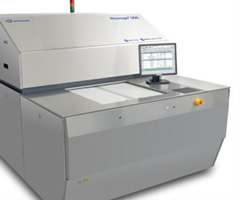
ORBOTECH LTD. has announced that Elekonta Marek GmbH & Co.KG., a European PCB manufacturer of MLB prototypes and QTA, has been successfully using the new Orbotech Diamond 8 Direct Imaging (DI) system for solder mask at its production facility in Gerlingen, Germany. This order was received and delivered during the third quarter 2015.
Orbotech Diamond 8 speeds up the solder mask production process for even the most complex designs. The driving force behind the system’s increased throughput and precise solder mask imaging is Orbotech’s unique SolderFast TechnologyTM. Utilizing a powerful light source engine, Orbotech Diamond 8 ensures consistent, high quality imaging, overcoming the most challenging surface topography variations as well as any distortions or abnormalities.
“As a market innovator in PCB prototyping, we are dedicated to continuously improving our production of sophisticated designs,” stated Mr. Lars Presche, General Manager of Elekonta Marek. “The high accuracy of Orbotech Diamond 8 solder mask DI has enhanced our ability to produce such designs, even those as small as 50µm. The system covers 100% of our production using a wide variety of solder mask types. This and other innovations from Orbotech have already boosted our throughput on unique and very complex prototypes.”
“With their reputation for bringing advanced solutions to their customers, it’s no surprise that Elekonta Marek is among our first European customers to have purchased and deploy the Orbotech Diamond 8,” said Mr. Hadar Himmelman, President of Orbotech West. ”We look forward to continue working together with Elekonta Marek, a long-time Orbotech customer, and supporting their needs well into the future.”
About Orbotech Diamond 8
Orbotech Diamond 8 is a fast, accurate solution for high-volume solder mask DI. Powered by Orbotech SolderFast Technology, Orbotech Diamond 8 is especially suited for designs with high complexity. Building on vast field-proven experience in patterning, the Orbotech Diamond 8 improves throughput, yield and productivity while decreasing total cost of ownership (TCO).
Orbotech SolderFast Technology employs a controlled wide UV spectrum to ensure fast throughput and high quality on a variety of solder resists. Unique one-pass exposure enables uniform solder mask imaging over the entire panel. Orbotech Diamond 8, with its sophisticated optical mechanism, including a patented light source with high energy illumination, enables high DOF (Depth-of-Focus) for consistent, precise imaging quality thus overcoming the most challenging surface topography variations as well as any distortion or abnormality. The system also offers advanced scaling modes for high precision registration, further improving throughput. Orbotech Diamond 8 delivers the most advanced image quality with no need to deploy an autofocus mechanism.
About Orbotech Ltd.
Orbotech Ltd. is a global innovator of enabling technologies used in the manufacture of the world’s most sophisticated consumer and industrial products throughout the electronics and adjacent industries. The Company is a leading provider of yield enhancement and production solutions for electronics reading, writing and connecting, used by manufacturers of printed circuit boards, flat panel displays, advanced packaging, micro-electro-mechanical systems and other electronic components. Virtually every electronic device is produced using Orbotech technology. For more information click here.


