


 Dan’s Biz Bookshelf: Four Important Books You Need to Read (Not Just Say You Have)
 The Marketing Minute: Cracking the Code of Technical Marketing


What Screens are Made of: New Twists (and Bends) in LCD Research
April 20, 2016 | LBLEstimated reading time: 4 minutes
Liquid crystals, discovered more than 125 years ago, are at work behind the screens of TV and computer monitors, clocks, watches and most other electronics displays, and scientists are still discovering new twists—and bends—in their molecular makeup.
Liquid crystals are an exotic state of matter that flows like a fluid but in which the molecules may be oriented in a crystal-like way. At the microscopic scale, liquid crystals come in several different configurations, including a naturally spiraling “twist-bend” molecular arrangement, discovered in 2013, that has excited a flurry of new research.
Now, using a pioneering X-ray technique developed at the U.S. Department of Energy’s Lawrence Berkeley National Laboratory (Berkeley Lab), a research team has recorded the first direct measurements confirming a tightly wound spiral molecular arrangement that could help unravel the mysteries of its formation and possibly improve liquid-crystal display (LCD) performance, such as the speed at which they selectively switch light on or off in tiny screen areas.
The findings could also help explain how so-called “chiral” structure—molecules can exhibit wildly different properties based on their left- or right-handedness (chirality), which is of interest in biology, materials science and chemistry—can form from organic molecules that do not exhibit such handedness.
“This newly discovered ‘twist-bend’ phase of liquid crystals is one of the hottest topics in liquid crystal research,” said Chenhui Zhu, a research scientist at Berkeley Lab’s Advanced Light Source (ALS), where the X-ray studies were performed.
“Now, we have provided the first definitive evidence for the twist-bend structure. The determination of this structure will without question advance our understanding of its properties, such as its response to temperature and to stress, which may help improve how we operate the current generation of LCDs.”
Zhu was the lead author on a related research paper published in the April 7 edition of Physical Review Letters.
While there are now several competing screen technologies to standard LCDs, the standard LCD market is still huge, representing more than one-third of the revenue in the electronic display market. The overall display market is expected to top $150 billion in revenue this year.
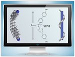
The individual molecules in the structure determined at Berkeley Lab are constructed like flexible, nanoscale boomerangs, just a few nanometers, or billionths of a meter, in length and with rigid ends and flexible middles. In the twist-bend phase, the spiraling structure they form resembles a bunch of snakes lined up and then wound snugly around the length of an invisible pole.
Zhu tuned low-energy or “soft” X-rays at the ALS to examine carbon atoms in the liquid crystal molecules, which provided details about the molecular orientation of their chemical bonds and the structure they formed. The technique he used for the study is known as soft X-ray scattering. The spiraling, helical molecular arrangement of the liquid crystal samples would have been undetectable by conventional X-ray scattering techniques.
The measurements show that the liquid crystals complete a 360-degree twist-bend over a distance of just 8 nanometers at room temperature, which Zhu said is an “amazingly short” distance given that each molecule is 3 nanometers long, and such a strongly coiled structure is very rare.
Page 1 of 2
Share on:


Testimonial
"The I-Connect007 team is outstanding—kind, responsive, and a true marketing partner. Their design team created fresh, eye-catching ads, and their editorial support polished our content to let our brand shine. Thank you all! "
Sweeney Ng - CEE PCBSuggested Items
Rules of Thumb: Design007 Magazine, November 2024
11/11/2024 | I-Connect007 Editorial TeamRules of thumb are everywhere, but there may be hundreds of rules of thumb for PCB design. They’re built on design formulas, fabricators’ limitations, and tribal knowledge. And unfortunately, some longtime rules of thumb should be avoided at all costs. How do we separate the wheat from the chaff, so to speak?
Connect the Dots: Best Practices for Prototyping
09/21/2023 | Matt Stevenson -- Column: Connect the DotsPCB prototyping is a critical juncture during an electronic device’s journey from concept to reality. Regardless of a project’s complexity, the process of transforming a design into a working board is often enlightening in terms of how a design can be improved before a PCB is ready for full production.
The Drive Toward UHDI and Substrates
09/20/2023 | I-Connect007 Editorial TeamPanasonic’s Darren Hitchcock spoke with the I-Connect007 Editorial Team on the complexities of moving toward ultra HDI manufacturing. As we learn in this conversation, the number of shifting constraints relative to traditional PCB fabrication is quite large and can sometimes conflict with each other.
Asia/Pacific AI Spending Surge to Reach a Projected $78 Billion by 2027
09/19/2023 | IDCAsia/Pacific spending on Artificial Intelligence (AI) ), including software, services, and hardware for AI-centric systems will grow to $78.4 billion in 2027, according to International Data Corporation's latest Worldwide Artificial Intelligence Spending Guide.
Intel to Sell Minority Stake in IMS Nanofabrication Business to TSMC
09/13/2023 | IntelIntel Corporation announced that it has agreed to sell an approximately 10% stake in the IMS Nanofabrication business to TSMC. TSMC’s investment values IMS at approximately $4.3 billion, consistent with the valuation of the recent stake sale to Bain Capital Special Situations.