


 It’s Only Common Sense: Be the Vendor They Compare Everyone Else To
 Marcy’s Musings: Additive Processes, Signal Consequences
 The Marketing Minute: If Your Marketing Budget Gets Cut in Half, Then What?


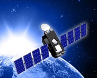
Stan Heltzel is a materials engineer working for the European Space Agency, and he is tasked with the job of procuring and qualifying PCBs that end up in satellites. I met with Stan at EIPC’s Summer Conference to discuss his presentation on qualifying a fabricator, his role at the ESA, and updating of space standards.
Barry Matties: Stan, please start by explaining a little about what you do.
Stan Heltzel: I’m a materials engineer at ESA and my responsibility is the qualification of printed circuit boards and the development of technology and qualifying the technology for space projects.
Matties: Everything you do is all about high reliability?
Heltzel: Yes.
Matties: You gave a presentation today on the qualification process, and talked a lot about the various approaches, the testing, and so on. What did you want the audience to take away from your presentation?
Heltzel: First of all, it’s the interaction between ESA, the national space agencies, contractors for satellite integration, and PCB manufacturers. They are working together in various organizational bodies and trying to address problems that no one organization could ever solve, so we’re doing that jointly. For instance, the nicest example I can think of is the cleanliness of the raw materials where PCB manufacturers were not in a position to ask for different quality standards from laminate suppliers until we got together as a group and addressed it all together.
Matties: Today you were showing some images of where you had peeled back the copper and found foreign debris in the mix. Is that something that’s commonly found, or is that an anomaly?
Heltzel: I think we should consider it an anomaly. We’re used to good quality materials that we get from laminate suppliers, but what we want is to be able to set the bar so we are able to distinguish between bad batches, if they oc casionally happen, and good ones. I don’t think it makes any sense to have inspection that does not discriminate between good clean materials and not-so-clean materials.
Matties: How do you even go about qualifying a fabricator to be a producer? What is it that you’re really looking for?
Heltzel: What’s important is that the qualified PCB manufacturer is committed to supply to the space industry for the long term. Then there are all kinds of technical requirements that are now written down in our standards, and for us to meet those technical requirements. Of course, some of these requirements are technically challenging to meet them 100% of the time. When we face problems, the really important thing is that we don’t give up. We should always have the mindset of continuous improvement and commitment to the space project to sort out any problems if they occur. I think that is one of the most important points to ESA.
Matties: Do you embed engineers from your agency into fabricator shops?
Heltzel: No, we do not.
Matties: You rely totally on their engineering and support to solve problems?
Heltzel: I audit PCB manufacturers. Also, the whole industry chain is involved with the quality assurance from PCB manufacturers, but inside those we do not have embedded engineers.
Matties: What is the greatest challenge in this whole process, from design to a completed board?
Heltzel: Mostly pricing, I’m afraid.
Matties: Really? I thought you had all the money you needed. It’s a government agency, right?
Heltzel: Let’s say the space project has a high budget, and it is an expensive business. But still, ESA does not buy the PCBs. It’s the industry buying the PCBs and the industry is pushing budget and they push back on PCB fabricators to provide a reliable PCB at a low cost. That is a conflict.
Matties: That sure is. The other aspect, of course, is that inspection is a standard step in almost every process for your application, I would imagine. That’s expensive, but necessary. A lot of people tell me, “If you have a process that’s in stable circumstances and you’re in control, you don’t need inspection.” It seems like that would be a mistake in this case.
Heltzel: It would be. We inspect a lot with regards to PCB procurement and PCB qualification. We are in the process of raising the bar in terms of the level of testing that we’re requiring and the number of inspections that we’re requiring. That work costs money but we justify that and we can quite easily convince industry that it’s just a fact that those inspections will then prevent failures later in the chain in manufacturing the product. Really, the expensive thing is when things go wrong and 20 people have to sit around the table once a week in a physical meeting to sort out the problems on schedule.
Matties: When things go wrong in the finished product, it’s hundreds of thousands of miles away perhaps, with no chance of repair.
Heltzel: When I speak about when things go wrong, it’s still ground-based.
Matties: That’s where you want to catch it.
Heltzel: You want to catch it before that. At the PCB level, you want to catch mistakes before they’re being assembled. It’s very late if we are catching things when we are performing ground-based environmental testing on the unit or even worse on the satellite. Keep in mind that these tests are also pretty severe tests of any electronic equipment that is passing, like a thermal vacuum campaign on the ground is expected to do well up in space.
Matties: Who’s doing your circuit design? Is that an internal function or is that farmed out?
Heltzel: That’s the industry’s responsibility— the OEMs.
Matties: So you basically go in and say, “We need something that gives us this functionality.”
Heltzel: Yes.
Page 1 of 2


