-

- News
- Books
Featured Books
- smt007 Magazine
Latest Issues
Current Issue
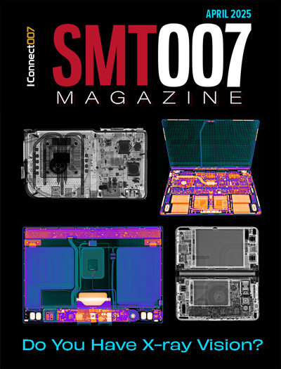
Do You Have X-ray Vision?
Has X-ray’s time finally come in electronics manufacturing? Join us in this issue of SMT007 Magazine, where we answer this question and others to bring more efficiency to your bottom line.

IPC APEX EXPO 2025: A Preview
It’s that time again. If you’re going to Anaheim for IPC APEX EXPO 2025, we’ll see you there. In the meantime, consider this issue of SMT007 Magazine to be your golden ticket to planning the show.

Technical Resources
Key industry organizations–all with knowledge sharing as a part of their mission–share their technical repositories in this issue of SMT007 Magazine. Where can you find information critical to your work? Odds are, right here.
- Articles
- Columns
Search Console
- Links
- Media kit
||| MENU - smt007 Magazine
Defect Features Detected by Acoustic Emission for Flip-Chip CGA/FCBGA/PBGA/FPBGA Packages and Assemblies
October 11, 2016 | Reza Ghaffarian, Jet Propulsion Laboratory, California Institute of TechnologyEstimated reading time: 4 minutes
The C-SAM (C-mode scanning acoustic microscopy) is the preferred method for finding "air gaps" such as delamination, cracks, voids, and porosity. This paper presents evaluations performed on various advanced packages/assemblies especially flip-chip die version of ball grid array/column grid array (BGA/CGA) using C-SAM equipment. For comparison, representative X-ray images of the assemblies were also gathered to show key defect detection features of the two non-destructive techniques.
Acoustic Emission Technology
Electronic Packaging Trend
Previous generations of microelectronic packaging technology aimed mostly at meeting the needs of high-reliability applications, such as the ceramic leaded quad flat package (CQFP). Nondestructive wire bond pull at the package level and subsequent visual inspection for solder joint integrity at the board level were adequate for ensuring the quality of CQFPs. Consumer electronics are now driving miniaturization trends for electronic packaging and assembly; they introduce a vast number of area array packages. The array packages initially only had hidden solder joints under the bottom area of the package; now the flip-chip die within package also have hidden joints.
The hidden joints—both at package and assembly levels—added significant challenges to the inspectability and certainty of assuring integrity at the various microelectronics hierarchy levels. Another added complexity is the transition to using only Pb-free solder alloys. Suppliers of electronics packages either have or will soon transition to using Pb-free alloys in order to enforce restrictions on hazardous substances (ROHS) for electronic systems. The solder joint appearance for the Pb-free solder alloys is dull rather than shiny, as it is for the tin-lead eutectic solder, which will add confusion even if visual inspection is used inadvertently as a criterion for the quality of joint acceptance or rejection of a Pb-free solder joint.
Inspection of ball grid array (BGA) and column grid array (CGA) package/assembly, especially their flip-chip versions is challenging1, 2, 3, 4, 5. Nondestructive X-ray inspection became a new approach for ensuring the quality of area array packages and assemblies. Even though X-ray can detect the level of voids and bridges of solder joints hidden under packages, it become of less value for detecting solder attachment and underfill integrity of higher I/O (>1000 I/Os) packages with flip-chip die technology (such as FCBGA and FC-CGA; Figure 1). Ceramic substrates considered for high-reliability applications are heavier and less penetrable to X-ray radiation than plastic, making them even more difficult to inspect for this category of packages and assemblies.
Figure 1: Microelectronic trends for single packaging technologies including flip-chip BGA and CGA.
Acoustic Micro-imaging, C-SAM, and X-ray
Acoustic microscopes emit ultrasounds ranging from 5 MHz to more than 400 MHz, so that micrometer size resolution can be achieved6. Ultrasound that penetrates a sample may be scattered, absorbed or reflected by the internal features of the material itself. These actions are analogous to the behavior of light. Ultrasound that is reflected from an internal feature has traveled through the entire thickness of the sample, and is used to make acoustic images. At least three basic types of acoustic microscope have been developed. These are the scanning acoustic microscope (SAM), scanning laser acoustic microscope (SLAM), and C-mode scanning acoustic microscope (C-SAM).
C-SAM uses the same transducer to pulse ultrasound and receive the return echoes, meaning that the acoustic image can easily be constrained to a depth of interest. It has the ability to create images by generating a pulse of ultrasound focused to a pinpoint spot. The pulse is sent into a sample and reflected off of interfaces. The frequency of the pulse and design of the lens are chosen to optimize spot size resolution and depth penetration for each application. In the reflection mode of operation, the same transducer is used to send and receive the ultrasonic pulse. Return echoes arrive at different times based upon the depth of the reflecting feature and the velocity of sound in the materials. The operator positions an electronic gate to capture the depth of interest. The amount of ultrasound reflected at the interface is based on the differences in the materials at the interface. The more different the materials the more ultrasound reflected.
Similar to X-ray, acoustic microscopy is a non-destructive technique for visualization of defects, widely used in the production of electronic components and assemblies for quality control, reliability and failure analysis. Usually the interest is in finding and analyzing internal defects such as delaminations, cracks and voids, although an acoustic microscope may also be used simply to verify (by material characterization or imaging, or both) that a given part or a given material meets specifications or, in some instances, is not counterfeit. Acoustic microscopes are also used to image printed circuit boards and other assemblies.
The ultrasonic frequencies pulsed into samples by the transducers of acoustic microscopes range from a low of 10 MHz (rarely, 5 MHz) to a high of 400 MHz or more. Across this spectrum of frequencies there is a trade-off of penetration and resolution. Ultrasound at low frequencies (such as 10 MHz) penetrates deeper into materials than ultrasound at higher frequencies, but the spatial resolution of the acoustic image is less. On the other hand, ultrasound at very high frequencies does not penetrate deeply, but provides acoustic images having very high resolution. The frequency chosen to image a particular sample will depend on the geometry of the part and on the types of materials.
To read this entire article, which appeared in the September 2016 issue of SMT Magazine, click here.
Suggested Items
KYZEN Focuses on Aqueous Cleaning and Stencil Cleaning at SMTA Wisconsin
04/24/2025 | KYZEN'KYZEN, the global leader in innovative environmentally responsible cleaning chemistries, will exhibit at the SMTA Wisconsin Expo and Tech Forum, scheduled to take place Tuesday, May 6 at the Crowne Plaza Milwaukee Airport. KYZEN will be on-site to provide attendees with information about aqueous cleaning chemistry AQUANOX A4618 and stencil cleaner KYZEN E5631J.
SMTA Bridging the Skills Gap in Arizona
04/24/2025 | Marcy LaRont, I-Connect007One area where SMTA really excels is through its local chapters. On April 16, 2025, I-Connect007's Marcy LaRont attended the Workforce Breakfast during the SMTA Arizona Expo & Tech Forum in Mesa, which featured more than 50 electronics professionals from the local area, including defense OEMs, and others who were attending for the first time. Blackfox and Hyrel Technologies sponsored the event. The keynote presentation featured Sean Denny, a professor at Estrella Mountain Community College, who emphasized a clear need for skilled hand soldering technicians.
IPC Releases Version 2.0 of IPC-2591, Connected Factory Exchange, with Expanded Device Coverage and Smarter Data
04/23/2025 | IPCIPC announces the release of IPC-2591, Connected Factory Exchange (CFX), Version 2.0, the global standard for plug-and-play, machine-to-machine, and machine-to-system communication for digital manufacturing.
ViTrox Marks 25 Years of Innovation with Cutting-Edge Solutions at NEPCON China 2025 in Shanghai
04/18/2025 | ViTrox TechnologiesViTrox, which aims to be the World’s Most Trusted Technology Company, is proud to announce its participation in NEPCON China 2025, taking place from April 22–24, 2025, at Booth #1E45, Shanghai World Expo Exhibition & Convention Centre (SWEECC).
Indium Experts to Present on Power Electronics at PCIM Europe 2025
04/17/2025 | Indium CorporationAs one of the leading materials providers to the power electronics assembly and e-Mobility industries, Indium Corporation experts will share their technical insight and knowledge on a variety of industry-related topics throughout PCIM Europe, May 6-8, in Nuremberg, Germany.


