


 It’s Only Common Sense: Customer Service Is Sales in Disguise
 Dan’s Biz Bookshelf: ‘Dream First, Details Later
 Happy’s Tech Talk #40: Factors in PTH Reliability—Hole Voids


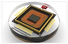
THz Camera Sees through Matter
March 10, 2017 | CEA LetiEstimated reading time: 1 minute
i2S recently worked CEA Tech to develop a terahertz camera prototype. THz rays do not pose any danger to the human body, opening up potential applications in a variety of fields.
Terahertz imaging could be a prime candidate for non-destructive testing. THz rays are non-ionizing and low-energy (from 0.3 THz to 10 THz), and have the capacity to penetrate a number of non-conductive and non-polar materials like skin, certain plastics, certain garments, paper, and cardboard. THz rays pose less of a danger than X-ray imaging systems and offer greater spatial resolutions than microwave or millimeter-wave scanners.
A microbolometer-based IR imaging technology developed by Leti, a CEA Tech institute, was used as the starting point for developing a 320 pixel X 240 pixel (50 micron pitch) THz imager—the current international state of the art in terms of sensitivity. The advance—which took the form of a high-performance THz camera prototype integrating the imager—was the result of joint R&D by i2S and CEA Tech.
The optomechanics and electronics were designed by i2S with Leti’s support. “This type of sensor can’t operate in the open air. Therefore, we had to place it inside a static vacuum enclosure to ensure good response capabilities,” said the Leti researcher in charge of packaging on the project. “We also had to give it a cover that would be transparent to these types of rays.”
At a frequency of 20 Hz, the camera prototype, when combined with the commercially-available THz light sources at the CEA Tech Optoelectronic Systems Integration platform in France’s Nouvelle Aquitaine region, can generate images of the contents of a cardboard box in real time. This type of camera will have potential uses in healthcare, security, NDT, and chemical testing for the farming and food industries.
Access to world-class THz resources in the region was a major factor that pushed i2S and CEA Tech to bolster their R&D partnership through a joint lab agreement to bring the camera to maturity. The CEA Tech Optoelectronic Systems platform offers manufacturers a unique environment for exploring this new imaging technique through feasibility testing for specific applications and the development of new solutions for manufacturers’ needs.
Share on:


Suggested Items
Japan’s OHISAMA Project Aims to Beam Solar Power from Space This Year
07/14/2025 | I-Connect007 Editorial TeamJapan could be on the cusp of making history with its OHISAMA project in its quest to become the first country to transmit solar power from space to Earth, The Volt reported.
OSI Systems Receives $34 Million Contract for Cargo and Vehicle Inspection Systems
07/11/2025 | BUSINESS WIREOSI Systems, Inc. announced that its Security division has been awarded a contract worth approximately $34 million by an international customer.
OSI Systems Lands $17 Million Order for Cargo and Vehicle Inspection Systems
07/07/2025 | BUSINESS WIREOSI Systems, Inc. announced that its Security division received an order valued at approximately $17 million from an international customer for cargo and vehicle inspection systems.
KYOCERA AVX Releases New 3DB Hybrid Couplers
07/04/2025 | PRNewswireKYOCERA AVX, a leading global manufacturer of advanced electronic components engineered to accelerate technological innovation and build a better future, released a new line of integrated thin film (ITF) hybrid couplers designed to facilitate the continued evolution of high-frequency wireless systems in industrial, automotive, telecommunications, and telemetry applications.
Driving Innovation: Direct Imaging vs. Conventional Exposure
07/01/2025 | Simon Khesin -- Column: Driving InnovationMy first camera used Kodak film. I even experimented with developing photos in the bathroom, though I usually dropped the film off at a Kodak center and received the prints two weeks later, only to discover that some images were out of focus or poorly framed. Today, every smartphone contains a high-quality camera capable of producing stunning images instantly.