


 SMT Perspectives & Prospects: Artificial Intelligence Part 6: Data Module 1
 Standard of Excellence: Overcoming Service Failures—The Art of the Apology
 Nolan’s Notes: Tariffs, Technologies, and Optimization


X-Ray Inspection of Lead and Lead-Free Solder Joints
July 31, 2017 | Glen Thomas, Ph.D., and Bill Cardoso, Ph.D., Creative Electron Inc.Estimated reading time: 13 minutes
ABSTRACT
X-rays are widely used to inspect solder joints in the electronics industry. Environmental concerns related to the impact of lead waste led the electronics industry to reduce or eliminate the use of lead in their manufacturing processes in 2007. Due to reliability concerns related to the use of lead-free solders in mission critical products, military and aerospace companies have been temporarily exempt from this requirement. However, as the availability of commercially available lead parts becomes scarce, some of the companies in the aerospace and military markets are considering the use of lead-free parts.
As aerospace companies consider the shift to lead-free solder alloys and glues, concerns have been raised about whether their current X-ray inspection and quality-control procedures will still be valid. With lead solder, joints are easily interpreted by the operator or the system imaging software because lead provides excellent image contrasts due to relatively high X-ray absorption compared to that of PCB and component materials. Will this hold true as they shift to lead-free solder compounds?
In this paper, we study how the physics of X-ray requires the change of settings and procedures for an accurate inspection. The atomic number of a material (Z) drives its X-ray absorption. Materials with high Z absorb more X-rays than materials with low Z. Tin (Z = 50), for example, is a common material found in lead-free solders. Lead, on the other hand, has atomic number 82. This difference in atomic numbers—and the different alloys present in the market today—may drive the need to change the settings and modes of the X-ray inspection system to match the chemistry of the solder joints. An accurate X-ray technique can only be achieved once the imaging system can produce similar contrast for both lead and lead-free solder inspection.
INTRODUCTION
It has been over a decade now since environmental concerns over contamination due to lead waste led the electronics industry to migrate solder processes away from the usage of eutectic tin-lead solder and towards utilization of lead-free compounds. Such a process change had several ramifications. The first major impact in the industry was the initial investment in equipment and materials to adapt to RoHS requirements. Another critical impact was the necessity to redesign reflow processes to bring the new assemblies with lead-free solders to an equivalent yield as the industry experienced prior to the migration to lead-free.
Although most companies have successfully moved to lead-free SMT lines, a considerable portion of manufacturers working in aerospace and military programs are still required to use lead solder. These companies routinely use X-ray inspection systems to assess and validate the quality of their assemblies. However, an X-ray inspection system will only be useful in a lead-free world if the changes in solder compounds do not have a significant deleterious effect on its imaging characteristics. To mitigate the concerns related to the inspection migration from lead to lead-free solder, in this paper we provide theoretical and practical studies of some of the effects of lead-free solder on an X-ray imaging capability. This is done primarily by comparison of X-ray attenuation properties for eutectic tin-lead solder and various lead-free solder compounds. We additionally show both actual images of solder joints made with lead and lead-free solder pastes. The conclusion of this analysis is that we found little contrast variation when using lead-free solders, which implies little change in inspectability.
X-RAY GENERATION AND ATTENUATION
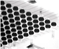
X-rays have been used for non-invasive high-resolution imaging of industrial and biological specimens since their discovery in 1895. Recently, a number of new contrast methodologies have emerged which are expanding X-ray's applications to functional as well as structural imaging. Figure 1 shows how the interaction of the X-ray photon with the atom inside the sample are leveraged by the different X-ray inspection techniques.
Figure 1: PTH process window by alloy.
X-rays are generated by accelerating electrons across a high voltage to collide with an anode composed of a high atomic number, high melting point material (commonly tungsten). Interactions between the electrons and the tungsten anode lead to the production of X-rays with a broad energy spectrum. The maximum energy of the X-ray spectrum is determined by the voltage applied in the X-ray tube. As tube voltage increases, the mean X-ray energy and number of photons produced both increase. This is demonstrated in Figure 2A for a tungsten anode operating at two different voltages: 80 and 140kV. The energy of the produced X-rays is an important determinant of their absorption by a given material. This energy spectrum can be modified by filtration through metal filters. Filtration is primarily used to increase the mean energy of the X-ray spectrum by removing low energy photons. Filtration can be used to both reduce radiation dose and improve image quality, and filtration can be optimized depending on the imaging[1]. Microfocus X-ray tubes used in high-end X-ray inspection machines have a small focal spot (area where the electron beam interacts with the anode), which reduces the source function blur (i.e., penumbra blurring) and thereby greatly improves the maximum image resolution. This increased resolution is necessary for imaging small features in electronic assemblies.
Figure 2: X-ray production and attenuation. (A) X-ray energy spectra produced at two different tube voltages: 80 and 140kV. Both the number of photons produced and the mean energy of the spectrum increases with higher voltage. (B) X-ray attenuation as a function of X-ray energy for multiple materials. In general, the X-ray attenuation rapidly drops with increasing X-ray energy. At the K-edge of each material, there is a sharp rise in attenuation due to the photoelectric absorption at that energy.
Page 1 of 5
Share on:


Testimonial
"The I-Connect007 team is outstanding—kind, responsive, and a true marketing partner. Their design team created fresh, eye-catching ads, and their editorial support polished our content to let our brand shine. Thank you all! "
Sweeney Ng - CEE PCBSuggested Items
Indium to Showcase High-Reliability Solder and Flux-Cored Wire Solutions at SMTA International
10/09/2025 | Indium CorporationAs one of the leading materials providers in the electronics industry, Indium Corporation® will feature its innovative, high-reliability solder and flux-cored wire products at SMTA International (SMTAI), to be held October 19-23 in Rosemont, Illinois.
‘Create your Connections’ – Rehm at productronica 2025 in Munich
10/08/2025 | Rehm Thermal SystemsThe electronics industry is undergoing dynamic transformation: smart production lines, sustainability, artificial intelligence, and sensor technologies dominate current discussions.
Amplifying Innovation: New Podcast Series Spotlights Electronics Industry Leaders
10/08/2025 | I-Connect007In the debut episode, “Building Reliability: KOKI’s Approach to Solder Joint Challenges,” host Marcy LaRont speaks with Shantanu Joshi, Head of Customer Solutions and Operational Excellence at KOKI Solder America. They explore how advanced materials, such as crack-free fluxes and zero-flux-residue solder pastes, are addressing issues like voiding, heat dissipation, and solder joint reliability in demanding applications, where failure can result in costly repairs or even catastrophic loss.
SASinno Americas Introduces the Ultra Series
10/07/2025 | SASinno AmericasSASinno Americas has introduced the new Ultra Series, the latest generation of offline selective soldering systems. Available in two models—the Ultra-i1 and Ultra-i2—the new series is designed to meet the needs of manufacturers running small to medium batch sizes, multiple product types, and frequent line changes, while maintaining exceptional precision and process control.
Elmotec by E-Tronix to Showcase SolderSmart® TOP Robotic Soldering at The Assembly Show 2025
10/06/2025 | ELMOTECE-tronix, a Stromberg Company, is pleased to announce its participation at The Assembly Show 2025 in Rosemont, IL, October 21st through 23rd. Exhibiting under Elmotec by E-Tronix, Booth #448, the team will highlight the SolderSmart® TOP robotic soldering system, featuring live demonstrations throughout the show.