


 Trouble in Your Tank: Understanding Interconnect Defects, Part 1
 It’s Only Common Sense: Marketing Isn’t Fluff, It’s Ammunition
 Driving Innovation: Mechanical and Optical Processes During Rigid-flex Production


Rick Almeida Discusses DownStream's Latest News
December 12, 2018 | Pete Starkey, I-Connect007Estimated reading time: 9 minutes
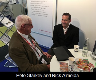
At the 2018 electronica exhibition in Munich, Rick Almeida, founder of DownStream Technologies, sat down with me to discuss the company’s latest news.
Pete Starkey: Rick, I think almost exactly two years ago we sat down and talked about building the interface between the designer and fabricator. I've seen news recently about your 2018 release including BluePrint-PCB and CAM350/DFMStream. Could you bring me up to speed with those?
Rick Almeida: Sure. So, this is the largest release in DownStream's history that we've worked on. The major theme around the release is bringing 3D technology into the back end of a design chain. It's used widely in mechanical CAD and is being heavily adopted now in ECAD. Our thoughts with 3D were twofold. If the designers were already doing a 3D design, we didn't want them to always have to go to 2D for post-processing, so we wanted to maintain the continuity of 3D throughout the design flow. For us, 3D was also a little bit of a different purpose where instead of modeling the design data in 3D, what we're doing is modeling manufacturing outputs in 3D. A designer can export Gerber and drill files, read them into CAM350 or DFMStream, add dielectric materials, assign thicknesses, and model the board as it would appear coming back from the fabricator.
Many years ago when I was a designer, you would do your designs, go out and get photoplots, and you would always have to imagine what the PCB was going to look like; you'd never see it until it arrived back from the fabricators.
Starkey: And the fabricator had to imagine what the designer was thinking. There just wasn't that interface.
Almeida: Right, and with a 2D system, you're very limited as to how you can look at it. You can look at it top-down or bottom-up, but it's very difficult to discern any type of via technologies that are being used in there. It's harder to see the relationship between the artwork and the drill files, and 3D solves all that. You can now rotate it at any angle and spin it around. We put some specific PCB features in our 3D technology; for example, we can take negative data such as a solder mask or a plane, which is great for design purposes, and automatically convert that into positive data, so it looks like it would appear in the actual printed circuit board.
Another key thing that we do is allow coloring not just by layers and objects, but by layer types. So, all the copper layers can be copper, and the solder mask screen or the silkscreen could be any color so that it appears like the actual PCB. What's nice about it as well is when we're running DFM analysis on it, we can probe the errors with both 2D and 3D, and the 3D view gives you a different perspective of what that DFM error actually would do to the copper clad itself in the copper, so there are some unique advantages in that.
We also bring 3D technology to the PCB stackup; we bring it into the one-up design, and I think we're probably the first and only company that can model the entire stepped-up panel in 3D. Once we have all of these 3D models, we also use them in BluePrint-PCB to create 3D model-based documentation—not necessarily to replace 2D documentation, but to augment the types of drawing data typically delivered by engineering. In a drill or a fabrication drawing, you can add a bare-board model to that drawing as a reference of what you expect the design to look like when it comes back from fabrication, and more importantly, the fabricator can gain a better understanding of what the designer had in mind before they start fabricating.
It's the same thing with assembly. We can add these 3D assemblies into documentation and also bring in step information. If a designer wants to document not just the PCB but also the enclosure that it goes into, that information can come in STEP, and they can use that on their drawings as well. Then, we output it to Adobe using their 3D PDF output, so it becomes interactive documentation.
That's the key part of the release content altogether. We've also made a number of productivity enhancements to CAM350 as far as changing the user interface to bring it up to more current standards and made it a little more dynamic and easier for people to work around the product. We've redesigned over a 100 different dialogues, consolidated a lot of information, and flattened out the user interface that users can be more productive with our products.
Starkey: You have a very large user base. How is this new release been adopted? Is it something that people have been waiting for?
Almeida: What's interesting is it just started shipping in early November, so users are still in the process of downloading and installing it. Our beta customers seem pretty happy with the direction that we were going in, so the feedback is very positive.
Starkey: That's great. So, how many users do you have worldwide?
Almeida: We have about 7,000 users worldwide who use the product.
Starkey: That's pretty impressive.
Almeida: And that's between both CAM350 and Blueprint, but CAM350 has been around for a long time; it's probably the most widely used CAM tool in the market.
Starkey: Forgive my ignorance, but in my day, there was effectively a big brick wall between design and manufacturing. I know you've been progressively knocking bricks out of that wall. Is there a barrier at all now, or is it all one continuous process?
Almeida: I think there still is a barrier there. One of the problems is that when you get into things like DFM, adding DFM into a design process typically means you lengthen the design process, which no one is ever keen to do unless they absolutely must. There's still a reluctance to do the analysis in the design side and pass it off to the fabricator to build because they’re going to build it either way. Things like ODB++ and IPC-2581 are going a long way to take out the bricks. We support both those interfaces because now instead of sending out a dozen different artwork files and drill files, it's one single file that has all the data in it, and it's all connected.
Page 1 of 2
Share on:


Testimonial
"Your magazines are a great platform for people to exchange knowledge. Thank you for the work that you do."
Simon Khesin - Schmoll MaschinenSuggested Items
Learning With Leo: UHDI—The Next Leap in PCB Manufacturing
11/05/2025 | Leo Lambert -- Column: Learning With LeoHigh density interconnect (HDI) technology has been a cornerstone of miniaturized electronics since Hewlett-Packard introduced the first chip-scale implementation in 1982. Over time, HDI processes became central to organic flip-chip packaging in the semiconductor industry. Today, the convergence of IC substrates and system-level PCBs has accelerated the adoption of UHDI.
BTU International Earns 2025 Step-by-Step Excellence Award for Its Aqua Scrub™ Flux Management System
10/29/2025 | BTU International, Inc.BTU International, Inc., a leading supplier of advanced thermal processing equipment for the electronics manufacturing market, has been recognized with a 2025 Step-by-Step Excellence Award (SbSEA) for its Aqua Scrub™ Flux Management Technology, featured on the company’s Pyramax™ and Aurora™ reflow ovens.
On the Line With… Ultra HDI Podcast—Episode 7: “Solder Mask: Beyond the Traces,” Now Available
10/31/2025 | I-Connect007I-Connect007 is excited to announce the release of the seventh episode of its 12-part podcast series, On the Line With… American Standard Circuits: Ultra HDI. In this episode, “Solder Mask: Beyond the Traces,” host Nolan Johnson sits down with John Johnson, Director of Quality and Advanced Technology at American Standard Circuits, to explore the essential role that solder mask plays in the Ultra HDI (UHDI) manufacturing process.
Rehm Wins Mexico Technology Award for CondensoXLine with Formic Acid
10/17/2025 | Rehm Thermal SystemsModern electronics manufacturing requires technologies with high reliability. By using formic acid in convection, condensation, and contact soldering, Rehm Thermal Systems’ equipment ensures reliable, void-free solder joints — even when using flux-free solder pastes.
Indium Experts to Deliver Technical Presentations at SMTA International
10/14/2025 | Indium CorporationAs one of the leading materials providers to the power electronics assembly industry, Indium Corporation experts will share their technical insight on a wide range of innovative solder solutions at SMTA International (SMTAI), to be held October 19-23 in Rosemont, Illinois.