


 Powering the Future: Why True Ceramic Circuits Are Not Just ‘Better PCBs’
 Global Sourcing Spotlight: The Global Quality Gap—Why Consistency Wins the Contract
 Knocking Down the Bone Pile: Precision Milling of Underfilled SMT Components


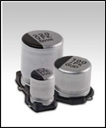
SMT electrolytic capacitors are a widely used component technology on IPC Class 3 avionics product designs. The body configuration of SMT electrolytic capacitors leads to solder joints that are only partially visible for optical inspection purposes. Figure 1 illustrates the obscured optical view of the capacitor lead due to the body construction/lead configuration. The capacitor lead exits from the bottom of the component and makes an "L" bend into the horizontal plane to provide surface area for the formation of a surface mount solder joint.
Figure 1: Typical SMT electrolytic capacitor. (Photo Courtesy of Panasonic)
Figure 2: Solder joint workmanship criteria: gull wing (top), and lug lead (bottom) per the IPC-JSTD-001 Specification.
Significant debate/discussion of whether this lead configuration falls under a gull wing or a lug lead optical solder joint acceptance criteria (Figure 2) had transpired. Two key questions generated during internal discussions of this issue were:
- Does the existence of a solder joint heel fillet impact the solder joint integrity?
- Does the height of the solder joint side fillet impact the solder joint integrity?
The entire solder joint workmanship discussion would be a moot point if it were possible to print a sufficient volume of solder paste to ensure that both an acceptable solder joint heel and side fillets are created. That approach is not a viable option since this large amount of solder volume would lead to solder joint bridging and capacitor placement defects.
Concerns with SMT electrolytic capacitors were not limited to Rockwell Collins. The IPC-JSTD-001 National Standard committee formed a task group to investigate and create solder joint acceptance criteria for SMT electrolytic capacitors. The JSTD-001 task group consisted of avionics/commercial electronic assembly producers and component suppliers. The task group created a proposed set of solder joint workmanship criteria for SMT electrolytic capacitors (Figure 3). Rockwell Collins was in general agreement with the proposed workmanship criteria except for the Minimum Heel Fillet Height (G (solder thickness under component lead) + T (thickness of the component lead)), which the internal discussions had highlighted as a solder joint attribute that required further investigation. Note 3 in the table below is just the solder thickness under the component lead.
The SMT electrolytic capacitor is a standard component that has been widely used on various avionics products for several years. Therefore, any concerns about whether the capacitors were meeting the Rockwell Collins solder joint workmanship criteria after years of production was more a case of a new product auditor raising the question rather than a solder reflow process change. Two years of SMT electrolytic capacitor defect data was plotted to identify any type of process/product/people change influences (Figure 4). Since no changes in the reflow soldering process or the component configuration were documented, the defect variation illustrated in Figure 4 is the result of subjective, inconsistent solder joint workmanship criteria visual inspection (i.e. the solder height expressed as a percentage of the lead thickness (T) – a solder side fillet height 1/4T or 1/2T or 1T?). A review of product field failure data for the SMT electrolytic capacitor found no reported defects in 10,000 opportunities over an 8 year time period.
Figure 3: IPC JSTD 001 initial draft of proposed workmanship criteria for SMT electrolytic capacitors (Credit: Jim Dagget, Raytheon and IPC JSTD-001 SMT Electrolytic Capacitor Working Group).
In conjunction with the IPC-JSTD-001 working group effort to create solder joint acceptance criteria for SMT electrolytic capacitors. Rockwell Collins initiated an investigation to determine solder joint critical attributes using thermal cycle conditioning and shear testing. The test results would be used to create a recommended set of solder joint acceptance criteria for proposed inclusion in the Rockwell Collins Workmanship Standards and consideration by the IPC-JSTD-001 working group.
TECHNICAL DISCUSSION
Test Plan
A test plan was created with a focus on two solder joint attributes: (1) the mechanical strength of the solder joint; (2) the thermal cycle fatigue strength of the solder joint. One of the primary reasons for having solder joint geometry and wetting criteria is to ensure the creation of a consistent, repeatable solder joint that can withstand the standard mechanical stresses of a product use environment. While the primary purpose of solder attachment of components is to provide an electrical connection, some mechanical characteristics are expected. Due to their geometry, electrolytic capacitors traditionally require additional mechanical strengthening, with the use of adhesive bonding for vibration or shock purposes. The use of adhesive bonding practices allows for reductions in solder joint geometry and wetting requirements. Shear testing was included in the test plan to demonstrate that the board pad attachment failure would occur before solder joint failure. Solder joint thermal fatigue testing was included in the testing as it represents the primary failure mode of solder joints in avionics applications. The electrolytic capacitors would be subjected to -55°C to 125°C thermal cycle conditioning followed by metallographic cross-sectioning to determine the level of solder joint cracking resulting from the global Coefficient of Thermal Expansion (CTE) mismatch induced by the thermal cycling.
Figure 4: Process inspection solder defects for SMT electrolytic capacitors for a two year period.
Test Vehicle
The test vehicle used in the investigation was a typical printed circuit assembly that contained 10 of the SMT electrolytic capacitors, making it an excellent candidate for testing (Figure 5).
Test Component
The SMT aluminum electrolytic capacitor analyzed in the investigation was representative of SMT electrolytic capacitors used in the industry. Rockwell Collins procures these components from various industry component suppliers (Figure 6, Figure 7). The pad configuration is similar between the various suppliers, so the resulting solder joints are very similar. Since these components are susceptible to failure due to vibration in the product use environment, an enhanced pad configuration (Figure 7, Anti-vibration) is occasionally used with supplemental silicone adhesive bonding.
Page 1 of 3


