


 The Government Circuit: Three Inescapable Conclusions About Global Trade Policies
 Global Citizenship: The Global Push for Digital Inclusion
 Knocking Down the Bone Pile: Addressing End-of-life Component Solderability Issues, Part 4


DDM Novastar to Introduce New Semi-Automatic Inspection System at IPC APEX EXPO 2019
January 28, 2019 | DDM Novastar Inc.Estimated reading time: 1 minute
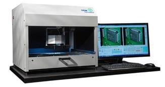
DDM Novastar Inc will launch its new NovaScope semi-automatic optical inspection system (SOI) at IPC APEX EXPO 2019 in San Diego (booth 1633, January 29-31). The NovaScope SOI System offers a ‘best in class’ solution that bridges the gap between manual PCB inspections and fully automatic AOI machines. This new versatile system offers fast and easy programming, automatic reporting, automatic photo documentation, reduced operator fatigue and optional side viewing.
The NovaScopeinspects and archives images of printed circuit board assemblies. It significantly increases the speed and accuracy of manual visual inspections, and it comes at a fraction of the price of a fully automated AOI. Programming can be done in a matter of minutes using the integrated Gerber, XY Placement List, and Bill of Materials import features. There is also a utility for simple matrix type scanning and inspecting of the board. Inspection area sizes range from 18” x 12” up to 24”x 18” and offer optional side view capability for oblique viewing in 8 programmable positions around each component.
The NovaScope is a powerful inspection tool for:
- High Reliability applications (MIL-Spec, Medical, Automotive)
- Hi-Mix, Low-Volume operations
- First Article Inspection
- Photo Documentation
- Conformal Coating
- Assembly Line Auditing
- Cleanliness / FOD/Tin Whisker detection
The system automatically moves a digital microscope to the inspection points, sets the lighting, camera height and angle, zooms to the region of interest, and displays a live image of the inspection area. The system displays a golden board image for visual comparison.
The images are automatically captured and can be stored as part of a post inspection report. The inspection can be done by component, by board region, or by a combination of both. Inspections can be performed for many reasons: verify part presence, rotation, polarity, registration, text, solder, solder paste, bent leads, bent pins, jumpers, cut traces, or any other top down or side visual feature on the PCB.
Available Options: In addition to options enhanced microscopes, and views, the systems can be configured as desktop unit or floor model, drawer or SMEMA conveyor, manual or programmable width control.
Share on:


Suggested Items
Silicon Mountain Contract Services Enhances SMT Capabilities with New HELLER Reflow Oven
07/17/2025 | Silicon Mountain Contract ServicesSilicon Mountain Contract Services, a leading provider of custom electronics manufacturing solutions, is proud to announce a significant upgrade to its SMT production capability with the addition of a HELLER 2043 MK5 10‑zone reflow oven to its Nampa facility.
Knocking Down the Bone Pile: Addressing End-of-life Component Solderability Issues, Part 4
07/16/2025 | Nash Bell -- Column: Knocking Down the Bone PileIn 1983, the Department of Defense identified that over 40% of military electronic system failures in the field were electrical, with approximately 50% attributed to poor solder connections. Investigations revealed that plated finishes, typically nickel or tin, were porous and non-intermetallic.
SHENMAO Strengthens Semiconductor Capabilities with Acquisition of PMTC
07/10/2025 | SHENMAOSHENMAO America, Inc. has announced the acquisition of Profound Material Technology Co., Ltd. (PMTC), a premier Taiwan-based manufacturer of high-performance solder balls for semiconductor packaging.
KYZEN to Highlight Understencil and PCB Cleaners at SMTA Querétaro Expo and Tech Forum
07/09/2025 | KYZEN'KYZEN, the global leader in innovative environmentally responsible cleaning chemistries, will exhibit at the SMTA Querétaro Expo & Tech Forum, scheduled to take place Thursday, July 24, at Centro de Congresos y Teatro Metropolitano de Querétaro.
Driving Innovation: Direct Imaging vs. Conventional Exposure
07/01/2025 | Simon Khesin -- Column: Driving InnovationMy first camera used Kodak film. I even experimented with developing photos in the bathroom, though I usually dropped the film off at a Kodak center and received the prints two weeks later, only to discover that some images were out of focus or poorly framed. Today, every smartphone contains a high-quality camera capable of producing stunning images instantly.