


 Standard of Excellence: Speed vs. Quality in Customer Service
 Knocking Down the Bone Pile: Revamp Your Components with BGA Reballing
 Global Sourcing Spotlight: Balancing Speed and Flexibility Without Sacrificing Control


Solder Mask Evolves into a Truly Additive Process
September 9, 2019 | John Fix, Taiyo America Inc.Estimated reading time: 3 minutes
As I write this article, it is the eve of high school graduation for my oldest son, Tom. It’s easy to reflect on his life that spans just short of 18 years. As parents, we all remember the milestones of our child(ren): when they were born and their first words, steps, days of school, etc. His high school graduation means he now embarks on the specialized educational path of his choice. For my wife and I, we have fantastic memories and look forward to seeing what Tom’s future holds.
I started with Taiyo America 18 years ago. And yes, 18 years can be a lifetime for some (like Tom), or short for others, like my wife and me. It’s all just a perception of time. Of course, technology can change significantly in a short period of time as well, which is not a perception; it’s a reality that we see every day. Changing technology has a dramatic effect on how we live our lives. As a young parent, I thought it was incredible to have a video baby monitor. Now, the norm is to have an app to monitor your baby’s every move from your smartphone. In the electronics world, 18 years have delivered changes from flip phones to smartphones, 2G to 5G, and plated through-holes to blind vias. In the automotive world, Tesla didn’t even start development until 2004; now, we have self-driving vehicles.
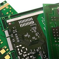
However, the 5G era is creating quite a bit of work for many PCB engineers as the materials required to keep up with the speed, frequency, and latency requirements need to be defined and qualified. Solder mask, for example, now becomes a truly additive process. There are several solder mask properties to investigate, including digital solder mask technology, process step removal, environmental extremes, heat management, crack reduction, and via filling, just to name a few. In this article, I will begin to explore the "hows" and the "whys" involved in making solder mask a strictly additive process.
Going Digital
One of the most important ones was the property function of imaging the material. PCBs have much tighter space requirements as devices get smaller and more processing is required that pushes PCB manufacturers to implement some form of digital printing into their process. Taiyo has spent several years in developing not only laser direct imaging (LDI) solder mask for the very popular Orbotech Paragon machine, but we have also designed direct imaging (DI) solder mask for various other DI equipment options that are now available.
These LDI/DI solder masks offer excellent advantages over traditional liquid photo-imageable (LPI) solder mask processes with regards to registration, tight tolerances, and fine dams. However, the true leap in digital solder mask technology is inkjet solder mask. For the past several years, Taiyo has worked with inkjet equipment manufacturers such as Orbotech and Notion Systems, just to name a couple, pushing this technology into the marketplace.
Inkjet solder mask allows you to enjoy the many advantages of LDI/DI, such as registration, no artwork generation or the waste/cost associated with it, and the capability to do fine features. You also gain the benefit of not leaving solder mask in the hole or on the pad because inkjet solder mask will never leave residue on pads or in the plated through-holes. This new solder mask application method truly becomes an additive process.
Process Optimization
In becoming an additive process, solder mask can now remove multiple steps in the current process. No more waste development solution that must be deposed of and no more artwork generations waste disposition. Tack drying and the associated solvent that is dissipated into the environment is gone. Thus, inkjet solder mask not only saves you money in processing cost, but you are making the environment greener. When would you have ever thought you would have heard that statement before—a PCB process that is environmentally friendly? Although the cost savings will vary from PCB manufacturer to manufacturer due to labor cost, markets served, board technology, etc., it is obvious there is money to be saved and opportunities to be taken.
To read the full article, which appeared in the August 2019 issue of SMT007 Magazine, click here.
Share on:


Testimonial
"The I-Connect007 team is outstanding—kind, responsive, and a true marketing partner. Their design team created fresh, eye-catching ads, and their editorial support polished our content to let our brand shine. Thank you all! "
Sweeney Ng - CEE PCBSuggested Items
BTU International Earns 2025 Step-by-Step Excellence Award for Its Aqua Scrub™ Flux Management System
10/29/2025 | BTU International, Inc.BTU International, Inc., a leading supplier of advanced thermal processing equipment for the electronics manufacturing market, has been recognized with a 2025 Step-by-Step Excellence Award (SbSEA) for its Aqua Scrub™ Flux Management Technology, featured on the company’s Pyramax™ and Aurora™ reflow ovens.
On the Line With… Ultra HDI Podcast—Episode 7: “Solder Mask: Beyond the Traces,” Now Available
10/29/2025 | I-Connect007I-Connect007 is excited to announce the release of the seventh episode of its 12-part podcast series, On the Line With… American Standard Circuits: Ultra HDI. In this episode, “Solder Mask: Beyond the Traces,” host Nolan Johnson sits down with John Johnson, Director of Quality and Advanced Technology at American Standard Circuits, to explore the essential role that solder mask plays in the Ultra HDI (UHDI) manufacturing process.
Rehm Wins Mexico Technology Award for CondensoXLine with Formic Acid
10/17/2025 | Rehm Thermal SystemsModern electronics manufacturing requires technologies with high reliability. By using formic acid in convection, condensation, and contact soldering, Rehm Thermal Systems’ equipment ensures reliable, void-free solder joints — even when using flux-free solder pastes.
Indium Experts to Deliver Technical Presentations at SMTA International
10/14/2025 | Indium CorporationAs one of the leading materials providers to the power electronics assembly industry, Indium Corporation experts will share their technical insight on a wide range of innovative solder solutions at SMTA International (SMTAI), to be held October 19-23 in Rosemont, Illinois.
Knocking Down the Bone Pile: Revamp Your Components with BGA Reballing
10/14/2025 | Nash Bell -- Column: Knocking Down the Bone PileBall grid array (BGA) components evolved from pin grid array (PGA) devices, carrying over many of the same electrical benefits while introducing a more compact and efficient interconnect format. Instead of discrete leads, BGAs rely on solder balls on the underside of the package to connect to the PCB. In some advanced designs, solder balls are on both the PCB and the BGA package. In stacked configurations, such as package-on-package (PoP), these solder balls also interconnect multiple packages, enabling higher functionality in a smaller footprint.