


 Standard of Excellence: Speed vs. Quality in Customer Service
 Knocking Down the Bone Pile: Revamp Your Components with BGA Reballing
 Global Sourcing Spotlight: Balancing Speed and Flexibility Without Sacrificing Control


Indium Corporation, Finetech Partner for MIT Integrated Photonics Bootcamp
February 11, 2020 | Indium CorporationEstimated reading time: 1 minute
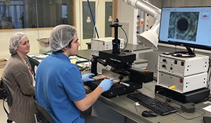
In January, Indium Corporation partnered with Finetech for MIT’s Integrated Photonics Bootcamp, a week-long, hands-on learning experience held at the MIT.nano facility in Cambridge, Mass., USA.
The training ran from Jan. 13-17 and allowed participants to explore and learn to solve problems using lab equipment, preparing them for the challenges to be faced in the workforce. Indium Corporation’s Andy Mackie, Senior Product Manager, and Meagan Sloan, Technical Support Engineer, met with students to talk about the chemistries and physical properties of bonding materials, and stressed the importance of using that information to select the right materials for their application.
“We were pleased to have the opportunity to partner with Finetech and MIT for this event,” said Mackie. “It provided us with the opportunity to educate students and industry participants, and to learn more about Finetech equipment capabilities and the specific materials needs of the photonics industry.”
Indium Corporation and Finetech’s session covered precision bonding fundamentals and featured optics, die and substrate temperature, alignment tolerances, thermal mismatch, inert atmosphere, and force. A review of bonding technologies included thermo-compression and thermo-sonic bonding, and UV adhesive cure.
Finetech provided a demonstration of flip-chip bonding using the FINEPLACER® lambda bonder. Participants learned about one of the most critical bonds in a complex surface mount photonic device—the assembly of QFN low-profile quad transceiver modules using thermo-compression bonding of a VCSEL onto a sapphire substrate. Each student had an opportunity to “drive” the equipment to get a feel for the sub-micron placement accuracy of the system.
Participants were fascinated to see and align such small features. Most couldn’t wait to get their hands on the machine and try the alignment process.
Indium Corporation is a premier materials manufacturer and supplier to the global electronics, semiconductor, thin-film, and thermal management markets. Products include solders and fluxes; brazes; thermal interface materials; sputtering targets; indium, gallium, germanium, and tin metals and inorganic compounds; and NanoFoil®. Founded in 1934, the company has global technical support and factories located in China, India, Malaysia, Singapore, South Korea, the United Kingdom, and the USA.
Share on:


Testimonial
"Our marketing partnership with I-Connect007 is already delivering. Just a day after our press release went live, we received a direct inquiry about our updated products!"
Rachael Temple - AlltematedSuggested Items
Sealed for Survival: Potting Electronics for the Toughest Environments
10/29/2025 | Beth Massey, MacDermid Alpha Electronics SolutionsElectronics deployed in harsh conditions face relentless threats from vibration, impact, chemical contaminants, airborne pollutants, and moisture, conditions that can quickly lead to failure without robust protection. Potting, the process of encapsulating electronics in a protective polymer, is a widely used strategy to safeguard devices from both environmental and mechanical hazards.
Driving Innovation: Mechanical and Optical Processes During Rigid-flex Production
10/28/2025 | Kurt Palmer -- Column: Driving InnovationRigid-flex printed circuit boards are a highly effective solution for placing complex circuitry in tight, three-dimensional spaces. They are now indispensable across a range of industries, from medical devices and aerospace to advanced consumer electronics, helping designers make the most efficient use of available space. However, their unique construction—combining rigid and flexible materials—presents a fundamental challenge for PCB manufacturers.
SMTAI 2025 Review: Reflecting on a Pragmatic and Forward-looking Industry
10/27/2025 | Marcy LaRont, I-Connect007Leaving the show floor on the final afternoon of SMTA International last week in Rosemont, Illinois, it was clear that the show remains a grounded, technically driven event that delivers a solid program, good networking, and an easy space to commune with industry colleagues and meet with customers.
ITW EAE Despatch Ovens Now Support ASTM 5423 Testing
10/15/2025 | ITW EAEAs the demand for high-performance electrical insulation materials continues to grow—driven by the rapid expansion of electric vehicles (EVs) and energy storage systems—thermal processing has become a critical step in material development.
Beyond Thermal Conductivity: Exploring Polymer-based TIM Strategies for High-power-density Electronics
10/13/2025 | Padmanabha Shakthivelu and Nico Bruijnis, MacDermid Alpha Electronics SolutionsAs power density and thermal loads continue to increase, effective thermal management becomes increasingly important. Rapid and efficient heat transfer from power semiconductor chip packages is essential for achieving optimal performance and ensuring long-term reliability of temperature-sensitive components. This is particularly crucial in power systems that support advanced applications such as green energy generation, electric vehicles, aerospace, and defense, along with high-speed computing for data centers and artificial intelligence (AI).