-

- News
- Books
Featured Books
- smt007 Magazine
Latest Issues
Current Issue
Intelligent Test and Inspection
Are you ready to explore the cutting-edge advancements shaping the electronics manufacturing industry? The May 2025 issue of SMT007 Magazine is packed with insights, innovations, and expert perspectives that you won’t want to miss.

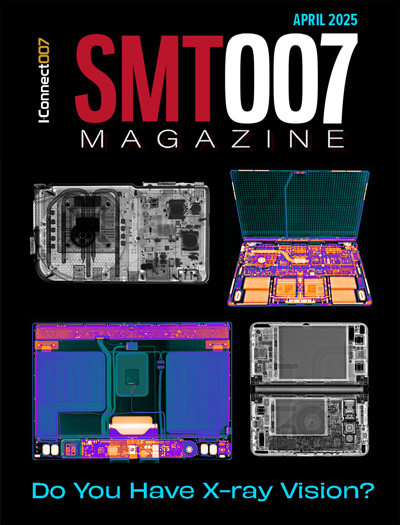
Do You Have X-ray Vision?
Has X-ray’s time finally come in electronics manufacturing? Join us in this issue of SMT007 Magazine, where we answer this question and others to bring more efficiency to your bottom line.

IPC APEX EXPO 2025: A Preview
It’s that time again. If you’re going to Anaheim for IPC APEX EXPO 2025, we’ll see you there. In the meantime, consider this issue of SMT007 Magazine to be your golden ticket to planning the show.
- Articles
- Columns
Search Console
- Links
- Media kit
||| MENU - smt007 Magazine
Design to Production Flow: DFT and Test Coverage Using Industry 4.0 Principles to Produce Good Products
December 1, 2021 | William Webb, ASTER TechnologiesEstimated reading time: 2 minutes
Achieving design for test (DFT) can be challenging for both design and test groups, as sometimes both expect that the other will be the one to manage DFT. The design and test groups might be in the same organization, or they could be an OEM vs. an EMS company. It works best if both the design and test groups are engaged in the process of DFT and trying to achieve the goal of the best test coverage and lowest rate of field returns.
Traditionally, design and test have operated in silos where there was not always the best communication, and at some point, the design was given to the test department to perform DFT. Often, due to project timelines and people working in different geographic regions, this means if some DFT concern was found, it may have been too late to address and resolve the issue. It is too late to wait until a board has gone through layout to begin DFT, as this needs to happen at the time of schematic capture, when the logic design is taking place, and before the board has gone for routing and layout. There are critical items that can be examined at the schematic capture phase to ensure that the board will be as testable as possible. A continuous feedback loop into DFT and test coverage understanding is key to producing defect free products at a minimum cost.
Companies must deliver good products to their customers, defect-free and at minimum cost. The challenge is how to detect or prevent defects from occurring so that only good products are shipped to the customer. Traditional DFT tools usually work only from the layout stage, which is too late in the whole process. Design data must be analyzed at the earliest stage possible in the product life cycle by importing schematic design data.
Electrical DFT rules violations should be identified and rectified prior to commitment to board layout, to prevent costly design re-spins. These rules can include standard and customer-specific checks relating to company requirements. With a centralized knowledge database, the same problems will never be repeated.
Test point requirements must also be identified pre-layout, during the schematic capture stage. This reduces the need for unnecessary test access, saving on PCB real estate, particularly on high density boards. The test strategy needs to be simulated, including any combination of inspection and test machines, delivering the highest test coverage. This unique combination provides electrical rules analysis, test point analysis, test strategy optimization, and test cost modeling based purely on schematic information. This, in turn, provides valuable layout guidelines that can be used to optimize the printed circuit board layout.
Once the PCBA layout is completed, a mechanical DFT analysis must be conducted to confirm the nets that require test access are not compromised by solder mask, component outline, adjacent probes constraints, etc.
To read this entire article, which appeared in the November 2021 issue of PCB007 Magazine, click here.
Suggested Items
Indium’s Karthik Vijay to Present on Dual Alloy Solder Paste Systems at SMTA’s Electronics in Harsh Environments Conference
05/06/2025 | Indium CorporationIndium Corporation Technical Manager, Europe, Africa, and the Middle East Karthik Vijay will deliver a technical presentation on dual alloy solder paste systems at SMTA’s Electronics in Harsh Environments Conference, May 20-22 in Amsterdam, Netherlands.
SolderKing Achieves the Prestigious King’s Award for Enterprise in International Trade
05/06/2025 | SolderKingSolderKing Assembly Materials Ltd, a leading British manufacturer of high-performance soldering materials and consumables, has been honoured with a King’s Award for Enterprise, one of the UK’s most respected business honours.
Knocking Down the Bone Pile: Gold Mitigation for Class 2 Electronics
05/07/2025 | Nash Bell -- Column: Knocking Down the Bone PileIn electronic assemblies, the integrity of connections between components is paramount for ensuring reliability and performance. Gold embrittlement and dissolution are two critical phenomena that can compromise this integrity. Gold embrittlement occurs when gold diffuses into solder joints or alloys, resulting in mechanical brittleness and an increased susceptibility to cracking. Conversely, gold dissolution involves the melting away of gold into solder or metal matrices, potentially altering the electrical and mechanical properties of the joint.
'Chill Out' with TopLine’s President Martin Hart to Discuss Cold Electronics at SPWG 2025
05/02/2025 | TopLineBraided Solder Columns can withstand the rigors of deep space cold and cryogenic environments, and represent a robust new solution to challenges facing next generation large packages in electronics assembly.
BEST Inc. Reports Record Demand for EZReball BGA Reballing Process
05/01/2025 | BEST Inc.BEST Inc., a leader in electronic component services, is pleased to announce they are experiencing record demand for their EZReball™ BGA reballing process which greatly simplifies the reballing of ball grid array (BGA) and chip scale package (CSP) devices.


