


 Nolan's Notes: The Next Killer App in Component Manufacturing
 The Knowledge Base: Unlocking the Invisible—The Critical Role of X-ray Technology
 Standard of Excellence: Turning Negative Customer Feedback Into Positive Outcomes


Step-by-Step
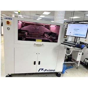
Step 4: Solder Print: 3D SPI and Process Control
December 31, 1969 |
Estimated reading time: 9 minutes
By Jean-Marc Peallat, Vi Technology
Solder paste inspection (SPI) becomes necessary to the SMT line as a process control tool, especially with small components' landing pads, such as the pads for microBGAs and 01005s. This article reviews the available SPI technologies (laser triangulation, Moiré methodology, flying absolute height profilometry), usefulness of SPI on the line, and the cost/benefit equation of adding solder paste inspection post-print.
For several years, process engineers and quality managers have queried the benefits of SPI. Despite the high level of defects associated with paste print, the implementation of SPI defect detection coverage has not been adopted widely on SMT lines. Many users still question the cost/benefit analysis. Other users consider that SPI, and especially 3D SPI, is critical during the new product introduction (NPI) phase or production ramp ups, but not of benefit during an established process. For them, the information provided by the SPI doesn't bring any relevant product quality improvements, or they feel ill equipped to leverage such improvements. At this stage, we surely need to re-explore the need for 3D SPI and consider the fact that volume calculation is enough to qualify the process.
With the advanced processes now demanding the use of smaller components such as 01005s, micro-BGAs, or package-on-package (PoP) components, it is clear that the use of in-process inspection becomes more important and could become a standard feature to ensure quality success. In this scheme, 3D SPI will assume a more important role in the test strategy.
The Solder Print ProcessThe solder paste print process is potentially very unstable, with more variation than any other SMT process. According to studies performed by numerous companies and universities, this process varies by up to 60%. The reason for this variation is the large number of process parameters involved. It is generally accepted that there are about 40 variables to control. These include, but are not limited to, paste type and formulation, environmental conditions, stencil type, stencil thickness, aperture aspect and area ratios, printer type, squeegee, print head technology, and print speed.
Stencil printer performance typically is quantified by measuring the transfer efficiency (TE) percentage and standard deviation of the paste deposition. Here, 100% would mean that the printed paste profile matches the calculated volume of the aperture opening. TE% varies on a typical SMT board between 20 and 130%. Transfer efficiency is generally better with rectangular apertures than square or circular ones; although, volume variations will exist when printing rectangular apertures in either vertical or horizontal orientations. The vertical apertures will print better and with a higher volume. The worst cases for print efficiency are small squares or round apertures less than 12 mil in diameter. Also of note is how the standard deviation increases as the TE% decreases. TE% decreasing indicates decreasing volume repeatability.
Some studies show that the volume of paste across an array package may not be as important as the consistency of all the pads in an array. Such that, as long as all of the pads have the same amount of paste, the resultant joints should be acceptable. However, if a few pads are under-printed compared to the others in the array, then poor joints may result.
3D SPI TechnologyLike automated optical inspection (AOI), the technology on which SPI is founded has not evolved significantly over the past decade. Until recently, there were two ways to inspect solder paste, one using the methodology of laser triangulation, and the other one based on Moiré technology. It is worthwhile to compare these two techniques and examine their respective advantages and disadvantages.
 Figure 2. Shadow effect.
Laser triangulation. Laser triangulation technology is combined with a 2D image to determine variance from standard. The height of the inspected object is given by the deviation of the laser trace (Figures 1 and 2). Laser triangulation drawbacks are mainly linked to a lack of resolution leading to poor accuracy. Moreover, having only one source (one laser), the exact value of the volume cannot be calculated. The phenomenon called "shadow effect" is due to geometrical layout of the system. The combination of single-angled laser beam and camera may produce a blind spot on the opposite side of the solder deposit to the laser (Figure 2).
In this area, the solder paste deposit is seen as square, as shown in Figure 2, and all the quantity of paste contained in this hidden volume (red zone) is not included in the measured volume. The error in the measurement value varies from shape to shape but can be up to 48% in the case of round apertures.
Using a laser to profile solder paste on a PCB is also subject to PCB color or finish variations. It requires a lot of program maintenance when facing such variations on the production floor.
 Figure 3. Moiré methodology.
Moiré methodology. Moiré topography is a method of tridimensional measurement by phase modulation. In this particular method, the lines projected on the object are modulated interference fringes, and by moving the observation grating, the height and volume of the object can be measured.
The drawbacks of the Moiré methodology are the lack of depth of field of view (more or less compensated by Z movement), the influence of noise and vibration in grating process, and the cycle time. The Moiré methodology is also subject to shadow effect if only one source of grating is used. Most systems available with Moiré have two modes of operation, providing speed of operation at reduced accuracy using one source or better accuracy at slower speed using two sources.
With Moiré technology, the inspection is made of a sequence of fields of view (FOV) with individual Z adjustment (the focus is made on average Z position in the FOV). From one FOV to the next one, covering the same array (BGA type), the references won't be the same and it may result in some differences in term of height or volume measurements. This may produce unreliable indicators of solder paste quality.
 Figure 4. FAHP methodology.
Flying absolute height profilometry. A new technology, flying absolute height profilometry (FAHP) combines the best features of both methods. It improves 3D SPI accuracy, speed, and depth of FOV. FAHP is a scanning solution using dual Moiré methodology. The board is scanned with a top-down camera using two structured light sources (from each side). The resulting image facilitates the calculation of both height and volume of paste, eliminating the shadow effect.
 Figure 5. PCB warpage measurement.
This technology, with a 6-mm FOV depth, allows an accurate measurement on all type of PCB, even compensating for high warpage values. During the scanning process, the system is able to measure the PCB profile itself and compensate for the warpage over the whole board (Figure 5).
 Figure 6A. PCB analysis without slope compensation.
The slope compensation (or warpage compensation), used at the pad level, provides higher height and volume accuracy (Figures 6A and B). Using the on-the-fly measurement technology facilitates a continuous measurement across the PCB, the height is referenced around the perimeter of the pad without the need for Z adjustment, eliminating potential errors.
With higher reliability, less dependency on board design or color, 3D SPI as a measurement system for small devices will became a useful tool to control the quality of the entire SMT process. In the 3D SPI world, to achieve accuracy and repeatability, the measurement system has to eliminate depth of field of view and warpage problems.
 Figure 6B. PCB analysis with slope compensation.
Getting More from Solder Paste InspectionToday, if the majority of engineers or managers are not convinced about the value of the 3D SPI, it is surely because the current solutions are not bringing enough valuable quality data. In other words, 3D SPI systems are checking for surface, height, or volume and are mainly qualifying deposit quality or stencil efficiency.
 Figure 7. Height/volume profile on BGA (105 pads).
With wide process tolerances, volume or height measurements don't appear as key drivers in reflow process and joint quality. For example, considering an area array component like a BGA with 105 connections (Figure 7), if the process window is set as minimum 40%/maximum 160% for height and volume measurements, you may end up with nearly 100% difference between the max and the min in the same array.
 Figure 8A. Height measurement distribution on BGA 105.
Considering the height values of the 105 pads and grouping them on the same graphic, the result should be a Gaussian curve centered on the average value and spread within 3 sigma. If the sigma value is low (narrow Gaussian curve), the solder paste distribution will be uniform through the array and the landing area will be seen as flat and good for device placement (Figure 8A).
 Figure 8B. Height measurement distribution on BGA 105.
If the distribution is very narrow around an average value of 110% with a few pads (2 or 3) with a very low value (50%), it may lead to bad joints or opens when the component will be placed and reflowed (Figure 8B).
In this case, all the pads are individually good within the process window, but the risk of poor quality is real. With such variation between deposits, when the device is placed and pressed on the board (landing area), the contacts will not be made evenly across the entire array. This increases the possibility of opens occurring in some areas. The same phenomenon can be observed for quad flat pack (QFP) or small outline (SO) type devices, when the solder paste is not equally printed. To compile these results, the 3D SPI system must be very accurate and should not depend on the measurement zone (warpage compensation).
In case of very small devices, such as 0201s and 01005s, beside the height and the volume, the shape of the deposit has to be considered as an important driver for final PCBA quality. While placing small devices, the contact surface between component and paste has to be maximized by the mechanical pressure made by the nozzle. At this stage, the shape of the deposits is a key mechanical factor and will affect the quality of the component placement and subsequent soldering. The shape has to be controlled and flagged as a warning prior to component placement. Then, by combining both solder paste and placement inspection, the system will be able to qualify the quality of the overall process before reflow.
3D SPI's Future in Process ControlWith software tools performing statistical process control (SPC) and closed-loop process control, the future lies in integrated systems able to manage the quality of the line from a process point of view. In a practical way, engineers increasingly are using SPC or managing data from inspection tools to control their process and tighten the process window. The current limitation of this approach is the lack of consolidation of the overall results gathered from the different inspection equipments and tests. Acknowledging that 3D SPI is bringing much more than height and volume measurements, such systems earn a spot as standard tools in the SMT process.
Today, the link between solder paste volume and joint quality on individual pads has not been proven. With a clear link between the quality of paste deposit at the component level and the quality of the soldering process, the value of 3D SPI systems escalates. The pad-to-pad volume calculation and the shape differentiator, combined with prereflow placement inspection, can guarantee sucessful soldering processes, circumventing X-ray inspection, which is costly and time consuming.
Driving process control and quality by controlling every step of the process is not impossible. It requires the ability to measure the right variables at the right process stage and consolidate them in such manner to provide relevant information. The future is in the use of the right level of inspection at the right stage and in the combination of the results.
Jean-Marc Peallat, marketing director, may be contacted at Vi Technology, St Egrève, France, jmpeallat@vitechnology.com.
Share on:


