-

- News
- Books
Featured Books
- smt007 Magazine
Latest Issues
Current Issue
Intelligent Test and Inspection
Are you ready to explore the cutting-edge advancements shaping the electronics manufacturing industry? The May 2025 issue of SMT007 Magazine is packed with insights, innovations, and expert perspectives that you won’t want to miss.

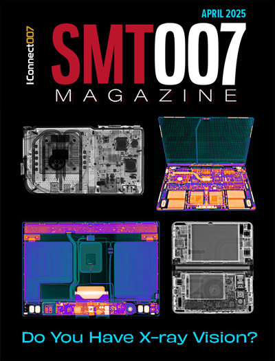
Do You Have X-ray Vision?
Has X-ray’s time finally come in electronics manufacturing? Join us in this issue of SMT007 Magazine, where we answer this question and others to bring more efficiency to your bottom line.

IPC APEX EXPO 2025: A Preview
It’s that time again. If you’re going to Anaheim for IPC APEX EXPO 2025, we’ll see you there. In the meantime, consider this issue of SMT007 Magazine to be your golden ticket to planning the show.
- Articles
- Columns
Search Console
- Links
- Media kit
||| MENU - smt007 Magazine
Process Optimization of an 01005
December 31, 1969 |Estimated reading time: 8 minutes
The ever-increasing demand for lighter weight, increasing functionality, and portability has led to size reductions of many component types. ICs have moved toward matrix-array connections with tiny pitches, and passive components have reduced to 01005 case sizes. This article documents an experiment conducted to determine process limits for these miniature components.
By Peter Grundy and Mats Magnell
The increasing demand for lightweight, full functionality, and portability has spurred the size reduction of many component types. ICs have moved toward matrix-array connections with small pitches, while passive components have shrunk to 01005 case sizes. Process windows for larger and wieldier components are well established, but process limits and comfort zones for these newer passive components are not. An experiment was conducted to investigate the process requirements for 01005 resistors and capacitors to determine solder paste printing parameters; accuracy and placement-force requirements; reflow soldering parameters; and pad shapes, sizes, and spacing.
 Figure 1. Comparative sizes of passive components. From left to right: 01005, 01005, 0201, 0603.
An experimental PCB was designed, and methodology used according to Design of Experiment (DOE) software.* Figure 1 shows the range of sizes of 01005 resistors and capacitors, while Table 1 shows their nominal dimensions.

null
Design of Experiment
The DOE software allows information to be gathered on the influence of SMT process parameters and pad sizes within a reasonable number of experiments.
Experiments can be conducted and planned to extract the maximum amount of information from the collected data, in the fewest number of experimental runs.
This project was comprised of two series of experiments, and some additional experiments. The aim of the first series of experiments was to identify important parameters and study how attachment quality changes with a specific parameter variation using only capacitors. Based on the feedback from the first series of experiments, a second series of experiments using capacitors and resistors was carried out with consideration taken to the focus on pad-size optimization. The aim of the additional experiments was to define the smallest component spacing and evaluate circular pads. In all experiments, manual inspection under a microscope assessed placements and joints, and results were judged according to the IPC-A-610C standard.
Components and Equipment
A PCB was designed with copper-pad (4,780 per PCB) for the 01005 components. It had a base material of FR-4 with an ENIG finish. Rectangular and circular pad shapes were designed, covering 160 different rectangular pad sizes and six circular pad sizes. In this experiment, length, width, and separation were defined as parameters that describe rectangular-pad geometry. Pad sizes were decided according to a worksheet that the software generated. On the left portion of the PCB, all possible rectangular pad sizes were laid out for the second series of experiments to optimize pad size. To study the smallest component spacing, pads with spacings ranging from 50 to 140 µm were designed in the middle of the PCB. To design a component clearance of 50 µm, pad width was designed to be 150 µm, because the copper-pad clearance below 100 µm was difficult to fabricate. Circular pads with diameters ranging from 200 to 300 µm were designed in the upper right area of the board.

An electroformed stainless-steel stencil, 0.75-mm thick was specified due to perceived small volumes of solder paste needed for 01005 pads. However, if the wall area-to-aperture ratio nears 1, there is a tendency for the paste to remain in the stencil, rather than transfer to the PCB. Pad ratios chosen were 0.57 (rectangular) and 0.67 (circular). Sn62/Pb36/Ag2 pastes with Size 4 and 5 particles were used. The paste was printed with 5-kg print pressure for Type 5, and 9-kg for Type 4. Components were placed using a pick-and-place machine** featuring a high-resolution camera, and the assemblies were reflowed using an oven with 5 preheat zones, 1 peak reflow zone, and 1 cooling zone. Both a linear reflow ramp <A> and a traditional soak ramp <B> were used. <A> and <B> are parameters used by the software. The software’s defining factors are shown in Table 2.
 Figure 2. Pad geometry parameters.
The first stage of the investigation is screening to identify important factors. After selecting screening as an objective, the DOE software generated a list that included several designs. It suggested a design with 70 experimental runs, each representing a unique setting of pad geometry and SMT process parameters. For quantitative factors, pad geometry parameters and values between the maximum and minimum were included as part of the experimental runs. For qualitative factors, SMT process parameters that switched between the two given options occurred in all experimental runs. After the design phase, 70 experimental runs in the worksheet were carried out. Defect numbers in each experimental run, according to each defect mode, were counted and entered into a software-generated worksheet.
Results and Observations: The First Run
Throughout experimental runs, there was no evidence of solder joint failure with side overhang, end overhang, end overlap, or maximum fillet-height criteria. However, the worst case of placement-side overhang, pre-reflow, was 30%. All components self-aligned under reflow, and it was concluded that the pick-and-place machine used was capable of placing 01005s to satisfy IPC-A-610C. It is known that lead-free solders have a higher surface tension than tin/lead, and that the tendency for self-alignment with lead-free paste is less. Pad length is the most significant factor, but proper consideration must be given to both pad width and solder paste type. The DOE software tends to generate maximum and minimum parameters for experimental runs, and it was noted that maximum pad length usually resulted in defects, no matter the other conditions.
High mounting force and small separation tend to cause more heel-fillet bridging. Solder paste Type 5 exhibits slightly better wetting ability than Type 4. Solder joint quality is similar with squeegee speed varying between 20 and 40 mm/sec., and reflow temperatures switching between profile <A> and <B>. Solder paste alloy composition can also influence joint quality. Spread and capillary forces that solder alloys exhibit have a direct effect on solder joint width and fillet height. If lead-free alloys were used, solder joints would be different because of their differing wettability factors.
Results and Observations: The Second Run
This experiment focused on pad-size optimization. Squeegee speed was fixed to 20 mm/sec., and the reflow temperature was fixed to profile <A>. Solder paste type and mounting force were found to have influence on some specific solder joint defects, so more experiments were designed to further test their significance. Experiments on the thickness of two components were designed to obtain optimum pad dimensions. Defect criteria were defined in the first experimental run. After inspection, optimum pad separation was defined as 160 µm, because perfect heel fillets were achieved, and there was no heel-fillet bridging. Figure 3 shows the defect rate as a function of pad size. Because size reduction is a main reason to use these small components, it is important to decrease pad size as much as possible to accommodate more components in the same board area. Defect rate decreases with increasing pad size, and 220 × 210 µm is the smallest pad size to obtain a 100% acceptable rate. It can be concluded that for 01005 capacitors, 210-µm pad length, 220-µm pad width, and 160-µm separation are the optimum pad dimensions to form an acceptable solder joint with the smallest area occupied on the board. Similar results were achieved by analyzing experiments on 01005 resistors. Optimum pad dimensions were found to be 190-µm length, 220-µm width, and 160-µm separation. The potential reduction in required board area compared to 0201 components is about 50%.
 Figure 3. Defect rates compared to pad dimensions.
Although Type 5 solder paste was judged to have a slightly better wettability than Type 4 in the first series of experiments, this may be because of the influence of smaller pads. On larger pads, there was no difference observed in the results between pastes. Type 4 solder paste usually costs less than Type 5, and is likely to be a better compromise. Component cracks occurred at placement forces of 3.5 N, which is borderline for capacitors, but outside the normal specification for resistors. Placement forces of 1 N are recommended.
 Figure 4. Bridging rate compared to spacing.
null
Results and Observations
For circular pads, it was observed that improved component self-alignment was obtained more often on circular pads than on rectangular pads. To achieve acceptable solder joints, pad diameter should be at least 260 µm. However, if these pads are used, a 01005 resistor occupies a PCB area of 0.1467 mm2, whereas the equivalent optimum rectangular pad occupies 0.1188 mm2. Circular pads for 01005 components do not contribute to any board-area saving, and are not recommended despite better self-alignment.
Minimum Spacing Between Components
Bridging can easily occur if printing settings are not optimized properly, particularly if the spacing is less than 100 µm. Solder paste wettability is another factor that influences the possibility to bridge after reflow. If lead-free solder alloys were used, more bridging could be expected due to the decreased wetting force compared to tin/lead. Figure 3 shows the bridging rate as a function of component clearance. No bridging between adjacent components was observed at a spacing of 100 µm. Therefore, 100 µm is recommended as the smallest component clearance.
Conclusion
A viable solder paste printing process for 01005 components can be achieved using a stencil with a thickness of 75 µm. A low mounting force of 1 N is recommended. With similar performance to Type 5 paste, Type 4 solder paste is recommended due to its lower cost. Optimum pad dimensions for 01005 capacitors and resistors were defined as 210-µm length, 220-µm width, 160-µm separation; and 190-µm length, 220-µm width, and 160-µm separation, respectively. The smallest component spacing is recommended to be 100 µm. If optimum pad dimensions are used, 50% of the board area can be saved compared to 0201 components. Components mounted on circular pads exhibited better self-alignment ability; however, circular pads cannot contribute to board-area savings.
* MODDE Design of Experiment software, www.umetrics.com.
** MY9 placement machine, MYDATA AB.
REFERENCES
For a complete list of references, please contact the authors.
Peter Grundy, director, P G Engineering, may be contacted at 44-1825-713155; e-mail: peter.grundy2@btinternet.com. Mats Magnell, marketing director, MYDATA AB, may be contacted at 46-8-4755762; e-mail: mats.magnell@mydata.se.


