


 Nolan’s Notes: Finding Your Sweet Spot
 Standard of Excellence: Delivering Excellence—A Daily Goal
 Knocking Down the Bone Pile: Tin Whisker Mitigation in Aerospace Applications, Part 3


Through-hole Assembly Options for Mixed-Technology Boards
December 31, 1969 |Estimated reading time: 6 minutes
This article describes three methods currently used for through-hole connector attachment on double-sided SMT PCBs: selective wave solder, pin-in-paste (PIP) reflow and solder preforms. A case study illustrates how the last method is an alternative when PIP provides insufficient solder.
By Ross B. Berntson, Ronald Lasky and Karl P. Pfluke
Selective wave soldering requires specialized equipment and processes to solder connectors. PIP reflow evolved as a way to accomplish through-hole assembly without additional equipment or process steps. In the PIP method, the additional solder required to fill the though-hole barrel is deposited by overprinting the pad in the area of each connector pin using standard SMT equipment. During reflow, the solder wicks to each pin, forming the solder fillet.

The task of determining the best board configuration for assembly is made increasingly difficult by tighter component densities, changing board thickness, more fine-pitch devices, changing surface finishes, greater power demands, increasing reliability concerns, upcoming lead-free technology, and more. These challenges are aggravated by ever-increasing demands for lower costs, which can be translated into greater throughput, fewer processes, less equipment and higher yields. A key obstacle to successful design and manufacture of mixed-technology boards, defined as containing double-sided SMT and pin through-hole (PTH) components is achieving an acceptable through-hole component solder fillet with reasonable yields, costs and process development. The tools available to the design and process engineer to overcome this obstacle will be outlined in this article, with particular attention on novel solutions (Table, p. 30).
Wavesolder Process
For assemblies with only a few SMT components on the bottom of the board, glue can hold the components in place prior to wave soldering. To avoid insufficient solder (shadowing) on these components, a glue-and-solder paste process may be required prior to the wavesolder step.
The use of pallets that shield bottom-side SMT components is common, especially when only the edge connectors require PTH soldering. This solution is increasingly difficult if the PTH components are dispersed throughout the printed circuit board (PCB). The advent of Pb-free wave and subsequent higher temperatures makes pallet management and full barrel fill more difficult.
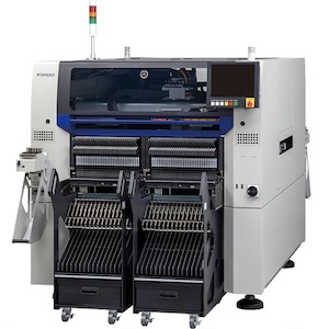
Selective wavesolder machines are becoming more common as assemblers tackle the challenges of more complex, mixed-technology PCBs. These systems incorporate an x-y table, sometimes z, which manipulates the PCB over a focused flux spray and a pin-point solder fountain.These systems offer flexibility and the ability to expose only desired regions of the board to flux, solder and heat. However, equipment costs, startup programming, space and process variability (especially with Pb-free solders) can mitigate some of the benefits. At the same time, this technology should become an increasingly attractive option.
Solder Paste Process
The typical PIP process is incorporated directly into the SMT process and offers advantages for mixed-technology boards with double-sided SMT and limited PTH requirements. These advantages include high throughput, current process and equipment use, and good yields. This PIP process requires:
- That the stencil be designed so that the correct amount of solder paste can be printed onto the through holes to form an acceptable joint after reflow
- The solder paste is amenable to the PIP process (usually Type 3 powder)
- The stencil printing process should be optimized
- The through-hole components are selected to withstand reflow soldering temperatures
- The through-hole component leads should be rounded at the end and of the correct length to form a good solder joint
- The through-hole components are correctly mounted
- The reflow profile is acceptable.
The greatest challenge in the PIP process is in designing a stencil that delivers an adequate amount of solder paste to the through-hole component. The geometry of an acceptable solder joint can be used to estimate the required solder paste volume. Solder paste is 50 percent solder by volume and 50 percent flux vehicle by volume. Solder paste rheology considerations, such as transfer efficiency, barrel fill and tackiness are critical to success. Pressurized print systems can improve barrel fill.
Numerous manufacturers have used the PIP process. Some shortcomings and ways of ensuring success include:
- Step stencils. When overprinting does not deliver adequate volume, a step stencil from 6 to 10 mil thick can be used. Solder paste transfer efficiency can be a concern because aspect ratios are not optimized. Also, sufficient holdout space to accommodate the stencil's non-planarity is required to avoid bridging or shorts.
- Dispensing solder paste. When residue levels are not a concern, dispensing solder paste can overcome printing limitations. As stated in the table, process and equipment support is a consideration.
- ICT test point. The large quantity of residue may limit the effectiveness of ICT and require test points or the use of a probe-testable solder paste. Introducing test points may further constrain the available overprint area.
Click here to download a .pdf of the table.
 Figure 2. Solder joints formed from PIP process.
A typical solder joint from an overprint with a 5-mil stencil is depicted in Figure 2. Note that the solder joints still have significant cavities, and flux residue limits inspection. In addition, the manufacturer of this assembly increased the overprint to such an extent that large solder beads can be found at via locations when the solder coalescence is not adequate to pull the solder into the joint. Increasing the solder paste barrel fill during printing was considered, but most of this solder paste is pushed out of the hole, and the pin design could no longer hold this paste.
Solder Preforms and Paste Process
New process development was required to eliminate defects associated with the current process, increase yields, ease inspection and improve quality while controlling costs. The solution was a combination of solder preforms and solder paste. Solder preforms (Figure 1) are stamped from rolled solder ribbon to the desired x-y dimensions, and are available in numerous shapes and sizes.
 Figure 1. Solder preforms are available in many shapes and sizes.
The solder preform process for through-hole connectors on mixed-technology boards uses current equipment and process expertise, including:
- Step 1. Solder paste is printed at the site of the connector pin. The solder paste deposit may be an overprint to provide a wicking path for the preform. For example, a preform can be placed in the overprint portion, and during reflow the preform solder will wick to the pin. Additional flux is not required because sufficient fluxing activity is available in the solder paste.
- Step 2. Preforms are placed in solder paste with automated placement equipment. The 0603 shapes, such as a washer or a 0603 segment are adaptable to high-speed placement from either tape-and-reel packaging or bulk feeding systems (Figure 3).
 Figure 3. Solder preforms are available in tape-and-reel and bulk packaging that integrates with high-speed assembly.
The manufacturer that supported this work was able to achieve results with the solder preform and solder paste solution, including:
- Easily inspected full barrel fill (Figure 4)
- No loss of throughput
- Elimination of step stencil with reduced defects at fine-pitch devices
- Reduction of overprint, which eliminated solder beads and balls
- Increased flexibility for future designs.
 Figure 4. The solder preform and solder paste solution delivered excellent through-hole solder joints.
Pre-fluxed solder preforms provide excellent PTH solder joints when combined with diode lasers and soft beam systems. This variation on the preform process does not require solder paste and works for temperature-sensitive components.
Conclusion
Mixed-technology circuit boards continue to challenge design and process engineers. Novel solutions, such as solder preforms and solder paste, linked array preforms, and selective solder machines should be considered for new designs and current assemblies.
References
For a complete list of references, contact the authors.
Acknowledgements
The authors would like to thank their customers who supported this project.
Ross B. Berntson; Ronald Lasky, Ph.D., PE; and Karl P. Pfluke may be reached at Indium Corp. of America, (800) 4-INDIUM; E-mail: RBerntson@indium.com, RLasky@indium.com and KPfluke@indium.com.
Share on:


