-

- News
- Books
Featured Books
- smt007 Magazine
Latest Issues
Current Issue
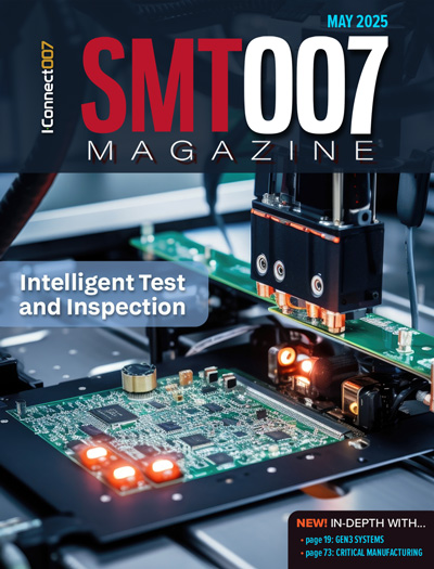
Intelligent Test and Inspection
Are you ready to explore the cutting-edge advancements shaping the electronics manufacturing industry? The May 2025 issue of SMT007 Magazine is packed with insights, innovations, and expert perspectives that you won’t want to miss.

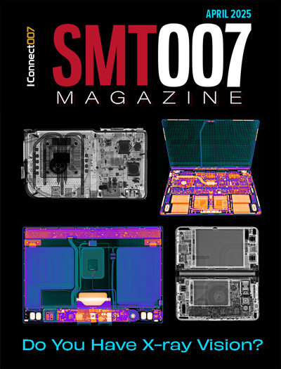
Do You Have X-ray Vision?
Has X-ray’s time finally come in electronics manufacturing? Join us in this issue of SMT007 Magazine, where we answer this question and others to bring more efficiency to your bottom line.

IPC APEX EXPO 2025: A Preview
It’s that time again. If you’re going to Anaheim for IPC APEX EXPO 2025, we’ll see you there. In the meantime, consider this issue of SMT007 Magazine to be your golden ticket to planning the show.
- Articles
- Columns
Search Console
- Links
- Media kit
||| MENU - smt007 Magazine
SMT Adhesive Deposition: The Line to Success
December 31, 1969 |Estimated reading time: 11 minutes
By Edward Fisher, Jay B. Hinerman and Douglass Dixon
Understanding and recognizing the options of different board configurations and adhesive dispense methods and regulations can improve and optimize SMT assembly processes.

Miniaturization is driving the design of new devices that use SMT components on both the bottom- and top-sides of printed circuit boards (PCB). Additionally, industry requirements for increased board reliability and faster throughput are stimulating demand for more robust board assembly processes, resulting in new manufacturing line configurations. This article investigates these line configurations along with the associated SMT adhesive requirements, process issues, dispense options and board design considerations. By understanding different board configuration options, adhesive dispense method options and adhesive requirements, engineers can improve and optimize their assembly processes.
Typical Manufacturing Line ConfigurationsThe board type being assembled dictates the appropriate manufacturing line configuration, the type of solder and adhesive used, as well as application methods. Five types of line configurations typically are used in PCB assembly.
Line 1 Traditional bottom-side line (Figure 1a). This line assembles bottom-sided boards with SMT and through-hole components. Most line configurations take the board assembly through pallet loaders and unloaders at the beginning and end of the process line. The wavesolder and manual assembly processes then are handled in a separate line that includes manual workstations and a wavesolder machine. Although very basic, this line builds reliable products when implemented correctly (Figure 1b).
The process:
- Apply adhesive
- Place components
- Cure adhesive
- Manual assembly/insert odd-form components
- Wave solder.
A traditional bottom-side line applies adhesive to a PCB, places components on the board and cures the adhesive, securing parts onto the board prior to wave soldering or manual assembly.
 Figure 1a-e. Five manufacturing line configurations that typically are used in PCB assembly.
After wave soldering, parts may be missing because of skipped or unacceptable adhesive dots, chipshooter placement errors, or damage that occurred during manual handling. By optimizing the adhesive dispense process, adding sufficient board support tooling in the manual assembly processes and controlling external forces on the assemblies, manufacturers can minimize missing components.
Line 2 Bottom-side line with solder paste application (Figure 1c). Like Line 1, this configuration assembles bottom-sided mixed-technology boards with SMT and through-hole components. However, Line 2 is more robust than Line 1 and uses a stencil printer to apply solder paste. The oven simultaneously reflows the solder and cures the adhesive, reducing the need to rework missing or insufficient solder on component leads. Manual assembly of odd-form components and board handling processes minimize missing parts. A separate wave solder process still is required for through-hole and odd-form components, which are inserted after the oven cure/reflow process.
The process:
- Apply solder
- Apply adhesive
- Place components
- Cure adhesive and reflow solder
- Manual assembly/insert odd-form components
- Wave solder.
In this application, adhesive dot height must be sufficient to contact the component above the solder paste deposition. Therefore, solder paste stencils must have reduced apertures (to print over a smaller area), and dispense nozzles must not allow the mechanical standoff to touch the solder pasted pads (if applicable).
 Figure 2. In the simultaneous double-sided reflow process, UV light cures the exposed adhesive fillet, providing sufficient adhesion for subsequent top-side component placement. The adhesive is fully cured during the solder reflow process.
Line 3 Mixed-technology top/bottom assembly with solder paste application (Figure 1d). Used to assemble top- and bottom-sided boards, Line 3 is fast becoming the preferred configuration for contract electronics manufacturers (CEM) because of the flexibility to run almost any board configuration from SMT to mixed-technology boards with through-hole and SMT components. Like Line 2, this configuration also uses solder paste to increase process yields for bottom-sided boards, contributing to process robustness.
The process:
- Apply solder (optional)
- Apply adhesive (optional)
- Place passive components
- Place fine-pitch components (optional)
- Cure adhesive or reflow solder
- Manual assembly/insert odd-form components
- Wave solder sent to separate line (optional).
More flexible than either of the previously discussed lines, this configuration provides greater reliability. Solder paste reflow reduces the number of parts missing from the assembly and minimizes wave soldering problems.
Flexible placement machines, which can be positioned at different locations in a manufacturing line, are capable of dispensing adhesive or solder, placing fine-pitch components, and simultaneously dispensing and placing. When configured to dispense and place components at the same time, these machines allow manufacturers to boost line capability and significantly maximize machine utilization. Flexible placement machines can be used in Lines 3, 4 and 5.

Line 4 Double-sided reflow soldering. During the reflow process, this line does not require adhesives to hold components to the board's bottom. Rather, the liquid solder has enough attraction to the metal surfaces of both the components and the solder pads to hold components securely. Line 4 is limited to boards with smaller components such as small passives and small-outline integrated circuits (SOIC) on the bottom-side assembly. Occasionally, adhesive will be added selectively to components that tend to tombstone or fall off during the second reflow process.
The process:
- Apply solder (optional)
- Apply adhesive (optional)
- Place passive components
- Place fine-pitch components (optional)
- Cure adhesive or reflow solder
- Manual assembly/insert odd-form components
- Wave solder sent to separate line (optional).
Line 5 Simultaneous double-sided reflow soldering (SDSRS) with ultra violet (UV) adhesives (Figure 1e). This relatively new process requires only one oven to simultaneously reflow the top- and bottom-sides of the board. SDSRS is appropriate for components from 0402 to 1206. However, there are some limitations with very large, heavy components on the bottom-side of assemblies.
The process:
- Print paste
- Apply adhesive
- Place components
- UV cure (5 to 30 seconds)
- Invert board
- Print paste
- Place components
- Reflow (3 to 4 minutes).
Adhesives that cure with UV light are key to this process. UV light cures the exposed adhesive fillet located on the component sides (Figure 2) and provides sufficient adhesion to hold the devices after the board is flipped for subsequent top side component placement. The adhesive fully cures during reflow, and the board is exposed only once to the reflow oven's high temperatures.
In all five line configurations, surface mount adhesives can be applied using syringe/pump dispense or via stencil printing. Specific throughput and adhesive requirements for the different board design configurations determine the preferred application method.
Syringe/Pump Dispense vs. Stencil PrintingSolder paste printing is used widely throughout the surface mount industry, yet many manufacturers who wave solder still use traditional dispensers when applying adhesive for bottom-side chip attach. With the increasing use of high-speed chip shooters and ever more complex boards, even the fastest adhesive dispensers struggle to keep pace.
 Figure 3. Modified reflow cycle for solder pasted pads accommodates simultaneous adhesive cure and solder reflow.
Standard adhesive dispensing, which currently is used in approximately 80 percent of all line configurations, is a continuous process where individual adhesive dots are deposited using pressurized syringes or pumps. This dispense method is highly flexible and easily allows for program changes in applications where board configurations are modified frequently. Syringe/pump dispensing is the only method of adhesive application possible when dots are placed after through-hole components are inserted into boards.
With chip shooters that place up to 80,000 components per hour, traditional adhesive dispensing can become the bottleneck in the manufacturing line. To match the accelerated component placement rates, multiple adhesive dispensers are required. Once a line requires two to three adhesive dispense machines, the cost can become prohibitive and stencil printing frequently becomes the more cost-effective dispense method.
Stencil printing provides an inexpensive, high-speed alternative that can deposit any number of adhesive dots simultaneously. For example, a board requiring 1,000 adhesive dots can be screen printed in just 30 seconds, while an adhesive dispenser running at 40,000 dots per hour will require one-and-a-half minutes. Stencil printing can provide any required dot shape with ease; single, double and multiple dots, squares or stripes also are easily produced. Single print thickness rarely is an issue, as most surface mount components are chip resistors, capacitors and other small devices with either a very small underside pitch or none at all (Table 1).
Adhesive RequirementsRegardless of the application method used, the rheological properties of adhesives play a major role in both dispensing and screen printing. Finding the correct combination of rheological properties can be the most important part of setting up a repeatable adhesive dispensing system.
 Figure 4. The wavesolder and solder paste pad designs have different adhesive dot size requirements.
Surface mount adhesives allow rapid and controlled dispensing, and form dots of a defined shape. To ensure that well-defined dot profiles are achieved and maintained post-dispense, adhesives are engineered to be thixotropic, thinning upon shear and thickening at rest. Surface mount adhesive viscosity decreases when shearing stress is applied during dispense, allowing easier flow. When the adhesive reaches the PCB surface, shearing forces are eliminated, and the adhesive quickly restructures and recovers viscosity.
Adhesives must exhibit high green or wet strength to hold the component prior to the curing process. Surface mount adhesive rheology is key in producing consistent dots with excellent green or wet strength. An adhesive with poor rheological properties will exhibit lower green strength and tend to form misshaped dots that can string, slump or lose contact with components.
SMT adhesives must be exposed to as little moisture as possible. Moisture in an adhesive dot will boil and explode violently during cure. This phenomenon, called "popcorning," causes voids that can weaken the joint and allow paths for solder to penetrate under the device. This may cause circuit shorting because of solder bridging. In a syringe, adhesives typically have an insignificant moisture level; however, when there is a long delay between dispensing and curing or when ambient conditions are very humid, the dispensed adhesive may absorb moisture. Moisture absorption can be a problem with stencil printing because of the large exposed surface area presented by open adhesive baths. To minimize this problem, most surface mount adhesives are formulated with raw materials that have low-moisture pick-up properties.
A modified oven profile allows adhesive to fully cure before solder reflow, ensuring that flux does not contaminate the adhesive during cure. Uncured, partially cured or contaminated adhesive can cause components to come off during the wavesolder process. A specialized cure cycle (Figure 3) consisting of a ramp rate of 2°C per second and a soak at the adhesive cure temperature is required for board designs using solder paste and adhesive. As the maximum adhesive cure temperature typically is around 150°C, curing SMT epoxy at typical reflow temperatures can embrittle the adhesive, which may lead to cracking and possible component loss during the wavesolder process.
 Figure 5. For adhesives applied on solder pasted pads, the preferred dot profile is tall and cylindrical.
Board DesignFor both stencil printing and standard dispensing processes, manufacturers must consider board design carefully, keeping in mind dot size requirements based on board layout pad design. Standard solder paste print pad designs usually have much smaller pad spacing than wavesolder pad designs. The processing method either solder paste or wavesolder designs has totally different requirements for adhesive between pads. A wavesolder pad design layout could have a dot size of 0.030" for an 0603 component, while a solder paste pad design layout could require a dot size of 0.015". (Figure 4)
Major processing issues involved in placing adhesive between solder pasted pads include: stencil design, dispense nozzle design, and adhesive dot profile.
 Figure 6. For wavesolder pad configurations, the preferred dot profile is "Hershey Kiss" shaped.
Adhesive dot profile is important when the solder paste process is added to a mixed-technology bottom-sided board, as solder pads can add 0.006 to 0.010" to the underside pitch between the components and the board.
After chip placement, the compressed adhesive dot must have a diameter smaller than the space between the solder pads, be tall enough to bridge the gap between the PCB surface and the body of the device, and adequately cover the component underside. The dot should not be so tall as to interfere with the component placement head. The adhesive gap (or dot height) is defined by the solder pad height above the PCB solder mask surface and the gap created by the difference in end metallization and device body thickness. Adhesive gaps/heights can vary from less than 0.05 mm for flat chips to more than 0.3 mm for large quad flat packs (QFP) (Figures 5 and 6).
 Figure 7. New packaging evolution trends create the need for mixed-technology lines that require different assembly processes and adhesive requirements.
In processes using solder paste on pads, getting a dot profile that does not touch the pads while still making intimate contact to the component underside may be difficult or even impossible. On smaller components, adhesive dots dispensed between solder paste pads tend to be tall and narrow, which can result in poor contact between the component and the adhesive. If board design prohibits good contact between the adhesive and components, double dots can be dispensed between the pads. Double dots effectively can increase adhesive volume under the component without encroaching on the solder paste pads. In some cases, a wavesolder pad design allows for larger dots between the pads.
Bottom-side assembly requires special stencil designs with reduced apertures to print the solder paste. The reduced aperture results in less solder paste being printed, which allows extra room for the mechanical standoff and dispense nozzle to touch down between the pads without contacting the solder paste. The smaller printed area also provides sufficient space between the adhesive and the solder paste to ensure that flux does not contaminate the adhesive during reflow.
ConclusionUsed in situations where boards are assembled with mixed-technology PCB designs, surface mount adhesives are necessary on assemblies with both through-hole and SMT components (Figure 7). The move to area array packaging drives the need for underfills, encapsulants and even surface mount adhesives on assemblies with SMT technology. In the future, designers that understand board configurations, dispense options and adhesive requirements will set up line configurations optimizing assembly processes.
EDWARD FISHER, applications chemist, may be contacted at Loctite Corp., 1000 Trout Brook Crossing, Rocky Hill, CT 06067; (860) 571-5100; Fax: (860) 571-2485; E-mail: ed.fisher@loctite.com. JAY B. HINERMAN, senior applications engineer, may be contacted at DEK USA Inc., 8 Bartles Corner Rd., Bldg. 200, Flemington, NJ 08822; (908) 782-4140; Fax: (908) 782-4774; E-mail: jhinerman@dek.com. DOUGLASS DIXON, dispensing product manager, may be contacted at Universal Instruments Corp., 147 Industrial Park Dr., Kirkwood, NY 13795; (607) 779-4630; Fax: (607) 771-8116; E-mail: dixond@uic.com.


