-

-
News
News Highlights
- Books
Featured Books
- smt007 Magazine
Latest Issues
Current Issue
Intelligent Test and Inspection
Are you ready to explore the cutting-edge advancements shaping the electronics manufacturing industry? The May 2025 issue of SMT007 Magazine is packed with insights, innovations, and expert perspectives that you won’t want to miss.

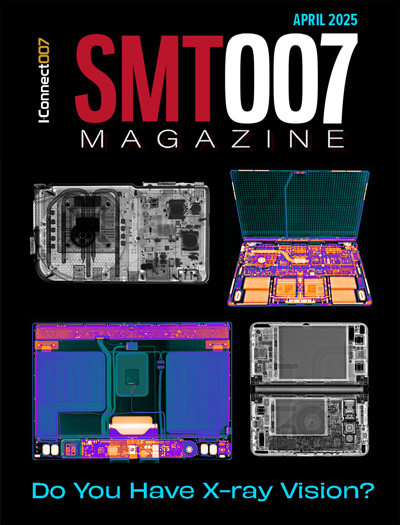
Do You Have X-ray Vision?
Has X-ray’s time finally come in electronics manufacturing? Join us in this issue of SMT007 Magazine, where we answer this question and others to bring more efficiency to your bottom line.

IPC APEX EXPO 2025: A Preview
It’s that time again. If you’re going to Anaheim for IPC APEX EXPO 2025, we’ll see you there. In the meantime, consider this issue of SMT007 Magazine to be your golden ticket to planning the show.
- Articles
- Columns
Search Console
- Links
- Media kit
||| MENU - smt007 Magazine
Machine Vision Placement Considerations
December 31, 1969 |Estimated reading time: 6 minutes
By Jeff Woolstenhulme and Evan Lubofsky
Although vision already plays a key role in the placement of surface mount devices, demands and expectations on system performance have grown significantly in recent years.

Machine vision's critical role in surface mount device (SMD) placement begins by locating printed circuit board (PCB) fiducial marks, assuring device alignment, and performing tolerance checking or inspection. More specifically, the vision system is responsible for locating and examining each lead to ensure that devices, including those with slightly deformed leads, are placed correctly, and those with missing, damaged or out-of-tolerance leads are rejected (Figure 1). These enhanced functions are the result of the smaller, more complex SMDs, devices' shorter lifecycles and proliferation of new device types. In fact, things are changing so fast that many companies designate employees to identify and define the new component types.
Accuracy and SpeedTo be viable, vision technology must improve placement performance while providing the necessary accuracy and robustness to handle shrinking device geometry and variability between manufacturers. This improved performance can lead to increased alignment yield, reduced operator intervention and increased mean-time-between-failure (MTBF). But, the vision technology also must provide processing speeds that meet increasingly higher placement speeds and throughput requirements, while developing customized placement guidance solutions. Finally, vision technology must enable engineers to do these operations in less time, increasing productivity and reducing time-to-market.
 Figure 1. In a typical component placement guidance application, the vision system uses an upward-viewing camera to "see" the underside of devices and a downward counterpart to capture fiducial and placement site images for board alignment.
System EvaluationNumerous advances in machine-vision technology are improving placement guidance performance. The following are questions to ask when evaluating a new system for SMD placement guidance:
- Can it locate PCB fiducial marks under a range of conditions? Because accurate, reliable PCB fiducial mark location is the first step in any SMD placement guidance application, the vision system must be able to "tolerate" degradations that can make a fiducial virtually unrecognizable. Variations caused by oxidation, tinning, wave soldering and other manufacturing processes can introduce specular reflections and surface inconsistencies that can alter a mark's appearance. Other problems that can affect a fiducial's appearance include board warpage, artwork stretch, excess solder build-up and board color changes.
- Can it locate nonstandard devices? While previous technologies mainly located rectangular devices, using nonstandard or odd-form components place greater demand on a vision system's capabilities. The new vision technology should reliably locate any device type, regardless of shape. To assist, software with built-in geometric pattern-matching algorithms can learn or "understand" an SMD's geometric attributes, locating the device reliably (Figure 2).
- Does it have reliable nozzle avoidance? SMD placers typically use front- or back-light illumination. Often, back lighting silhouettes the device. The resulting binary-like image makes device location easier. However, the pickup nozzle's silhouette often will protrude from behind the device or partially occlude small devices such as chips, which present a location-accuracy challenge for the vision system. While front-lighting techniques may prevent the silhouette problem, the nozzle's pixel gray values may hinder the system's ability to distinguish between the nozzle and device. A vision system capable of recognizing the differences between devices and the pickup nozzles that hold them is necessary (Figure 3). By tolerating partial nozzle occlusion, the enhanced system increases device alignment accuracy while preventing incorrect placement stemming from vision error. Some advanced placement-guidance packages are equipped with training tools that determine the nozzle's critical dimensions and the center of rotation. This information can improve the system's interference-avoidance capability, device location accuracy and inspection while detecting no- or miss-picks.
- Can it locate and inspect fine-pitch ball grid arrays (BGA), chip scale packages (CSP) and flip chips? Handling a range of device types is critical in many placement-guidance applications. However, to accurately locate and check lead tolerances on devices such as BGAs, random-patterned flip chips and CSPs, the vision system also must deal with device circuitry, which can create a visually confusing image. Similarly, the system should reliably locate devices with white ceramic surfaces, which can be overwhelming for traditional vision technologies with their low-contrast and reflective nature. Finally, advanced vision systems need to handle the current diverse range of components and future devices.
- Does it have automated tools for creating device descriptions? New vision software tools can automate creating device descriptions for components. Instead of manually entering parameters to create device descriptions from scratch, users can present a device to the vision camera, take its picture and automatically create a synthetic, computer-aided design (CAD)-like description. This can improve device description accuracy and speed-up description creation and test especially in situations where new devices frequently are introduced or where uniquely shaped components must be described. Lastly, vision systems capable of automating device description also may reduce operator errors.
- Does it support dif

Figure 2. Geometric pattern-matching algorithms enable machine vision to "understand" the geometric features of a uniquely shaped device, such as this radio frequency (RF) shield case.
Vision systems designed with an open software development environment can provide flexibility and control in placement-guidance applications. Such systems allow users to develop applications using turnkey inspection tools, C++ programming tools or a combination of both. Some systems permit users to incorporate their own custom vision algorithms.

Figure 3. Nozzle training tools "learn" the shapes of pickup nozzles by measuring their critical dimensions and the center of rotation, avoiding their interference.
With access to various software development tools, users have the power to build fully customized placement-guidance solutions based on their own requirements (see Sidebar).
ConclusionWhen evaluating machine vision systems for SMD placement guidance, a system capable of increasing alignment yield, throughput and possessing the flexibility to meet assembly market conditions is preferred. By selecting technology that achieves these objectives, new component types and device variability can be handled while simplifying processing.
JEFF WOOLSTENHULME is industry marketing manager and EVAN LUBOFSKY is senior writer at Cognex Corp., One Vision Drive, Natick, MA 01760-2059; (508) 650-3145, (508) 650-3140; E-mail: jeffwool@cognex.com and elubofsky@cognex.com.
Beyond Gray-scale RecognitionTraditional component placement vision systems rely on gray-scale normalized-correlation pattern-matching techniques as the basis for locating and inspecting devices. These methods rely on gray-value pixel grids to represent images, an approach that can have limitations when handling fine-pitch and odd-form devices.

Figure 1. The model image (a) shown in pixel grid, the run-time image rotated (b) and scaled (c). By analyzing the geometric information from both the images' features and their spatial relationships, GPM technology can determine a pattern's position regardless of its angle, size or appearance.
The main problem with pixel-grid representations, or models, is that they become less accurate when moved, rotated and scaled in sub-pixel steps. Small fractional movements cause the pixel-grid values to change, distorting the way the model image and run-time images line up, i.e., the patterns' "match position." Normalized-correlation-based pattern matching techniques typically locate patterns only with 0.250 to 0.100 pixel accuracy. Performance deteriorates if the device rotates and the part appears larger or smaller because of changes in optical settings or if lighting conditions vary.
Another problem can be poor image contrast. For example, traditional technologies have had difficulty locating leads on white-bodied devices because the device body and pickup nozzles often have pixel values similar to the leads. This can create a visually confusing scene for the vision system and prevent reliable lead location.
By contrast, most newer, advanced vision systems avoid these problems by using geometric pattern matching (GPM) technology. GPM converts the pixel-grid array provided by a camera to a geometric representation, so it can recognize devices or device patterns by their shape (Figure 1). For example, it might interpret a square as four line segments and a football as two arcs via a conversion process. First, it identifies and isolates the key features within an image and measures characteristics such as shape, dimensions, angle, arcs and shading. It then corresponds to the model image's spatial relationships between its key features to the run-time image, encompassing distance and relative angle. From that, the pattern match position can be determined by the vision system at an accuracy of up to 1/40th of a pixel even if the device is rotated, optical settings are off, lighting is inconsistent or there is poor image contrast.


