


 Standard of Excellence: Speed vs. Quality in Customer Service
 Knocking Down the Bone Pile: Revamp Your Components with BGA Reballing
 Global Sourcing Spotlight: Balancing Speed and Flexibility Without Sacrificing Control


Characterization of Solder Defects in Package-on-Package with AXI Systems for Inspection Quality Improvement (Part 1)
June 29, 2015 | Z. Feng, D. Geiger, W. Liu, A. Mohammed, M. Kurwa, Flextronics, and G. Tint, HDI SolutionsEstimated reading time: 5 minutes
Abstract
As a part of series of studies on X-ray inspection technology to quantify solder defects in BGA balls, we have conducted inspection of three-level Package-on-Package (PoP) by using a new automated X-ray inspection (AXI) technology that is capable of 3D-CT imaging. The new results are compared with the results of earlier AXI measurements. It is found that 3D measurements offer better defect inspection quality, and reduce lower false call and escapes.
Introduction
Package-on-Package (POP) devices are different from conventional SMT devices because they require solder attachments at different levels from the PCB surface. Their importance becomes even greater as PoPs are increasingly utilized in various types of assemblies because designers want to take advantage of 3D integration, to offer superior performances in their new products. Therefore, achieving the best possible PoP solder joint quality becomes important consideration for today’s PCBA manufacturers.
As solder joints in a PoP device cannot be inspected by optical means, X-ray inspection mostly is the only way to assure their quality nondestructively. Recently, automated X-ray inspection—AXI (AXI3, AXI4)—are found to have capabilities to detect not only solder bridge, missing ball, extra solder, and ball voiding defects, but also open/HIP for the bottom and top layers of POP. However, AXI images are not as clear as 2DX and planar CT (pCT). In this project, we used an AXI with pCT (AXI5) capability to characterize the solder defects in POP to explore improvement in inspection quality in a production environment.
The goal of this project is to evaluate the level of performance offered by different types of X-ray inspection equipment. It is better for the PCBA manufacturers to be able to test POP using AXI with pCT images. Getting unambiguous images with Pass/Fail result AUTO output are the obvious benefits. Our project consists of three phases: (1) Analytical comparison of images acquired by 2DX and AXI with pCT; (2) exploration of possibilities to optimize the AXI with pCT algorithms in order to improve the quality of defect detection; and (3) attempt to develop a process for AXI with pCT algorithm optimization.
Background
With more and more PoP packages in production assemblies, achieving zero defects escape rate came to our focus in recent years. In early 2013, we faced the issue that some open defective pins on the top layer of POP were escaped from AXI. Therefore, we have been working with our engineers and X-ray vendors for this issue being resolved. In 2013, the best detecting coverage for open/HIP on the bottom layer was 85% with about 14,000+ false call PPM, and was about 50% defects detecting coverage with >30,000 false call PPM for the top layer of POP. It was not available to detect open / HIP on top layer with 3 layers POP from our AXIs that time.
However with many efforts for new software development, as well as Algorithms Threshold settings studies, good achievements were obtained in 2014. Both AXI 3 and AXI 4 have capabilities to detect open/HIP defects with three-layer PoP packages, and the average defects escaped is 4-8% with about 20,000+ false call PPM. The challenge was that getting clear image difference between good solder and bad solder pins while showing big separation between good and bad joints numerical data as measured by main Algorithm.
There was benefit to verify POP solder joints with AXI capabilities. Since November of 2013, we have not seen any defective pin on 3 layers POP from our SMT lines at Milpitas site after SMT process improvement. With the real-time AXI testing data feedback, we are confident with our SMT process. Because of our AXI machine on the line with high false call PPM and not clear different X-ray images between good solder joint and bad solder joint, therefore usually we use 2DX to verify the defective pins which called at AXI. In this way, we do rework only when it is real defect.
Experiments
In this project, we use AXI 5 for POP X-ray inspection. The reason we choose AXI 5 is that it not only has AXI capabilities, but also offers CT capabilities at reasonably high speed. These features (AXI & pCT) should provide more benefits for our SMT lines.
1. Summary of Previous Experiments on AXI3, AXI4
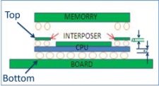
The inspection quality of AXI not only depends on the AXI machine design, but also on the on the structural complexity of a given POP. Figure 1 illustrates the three-layer POP we utilized in this study, which is assembled on a customer board. We do not test middle interposer ball layer of the POP on AXI as no SMT process is required on these pins. The POP structural information is tabulated in Table 1.
Figure 1: Structure of 3 BGA layers POP on Customer Board
- a1 (Substrate1) = 0.122 ±0.022 mm
- a2 (Substrate 2) = 0.262 ±0.022 mm
The 2DX results are adopted as the reference for this POP AXI study. We use two parameters (Defect Escaped % and False Call PPM) to evaluate the AXI capability. Table 2 summarized the results from inspections by AXI 3, and AXI 4. The definitions of Defect Escaped % and False Call PPM are expressed by Equation 1, and Equation 2.
Equation 1:
Defect Escaped % = (Total # of Defect Escaped / Total # of Defects) x 100%
Equation 2:
False Call PPM = (Total # of False Call / Total # of Tested Pins) x 1,000,000
The 2DX, AXI3, and AXI 4 testing results are shown with pin locations in Figure 2. The cell colors are described as below.
Figure 2: The Test Results of POP Board from 2DX, AXI3, AXI4
Figure 3: X-ray images for Detected HIP, Good solder, False Call pins from 2DX, AXI3, and AXI4.
Figure 3 shows X-ray images for Defective HIP, Good solder, and False Call pins on top BGA ball layer of the POP from 2DX, AXI3, and AXI4, where green, red, and yellow colors stand for Good solder joint, HIP/Open defective pin, and False Call pin respectively. It is obvious to see difference for good solder and open solder on 2DX images. Based on the observed images, the big challenge in AXI is that there is no obvious difference visible between the images of good solder joint verses defective HIP/Open pins. It is also observed at both AXI3, and AXI4 machines.
Therefore, our previous AXI study showed that AXI 3 and AXI 4 have capabilities to test POP including three ball layers by full AUTO mode with focus images for different BGA layers on POP Package. Both AXI3 and AXI4 have capabilities to detect POP open, HIP defects with some level of success. There is no clear visual distinction between AXI images of good verses bad pins, especially when it comes to HIP/Open defects. The requirement to balance for Defect Escaped % and False Call PPM was our main focus issue for AXI with POP study, and looking forward to having characterization of solder defects in POP with AXI systems for inspection quality improvement. That is the driving factor to work on with AXI 5 which has AXI and pCT capabilities for the POP project.
In Part 2, the authors discuss the highlights of AXI with planar computer tomography (pCT).
Editor's Note: This paper has been published in the technical proceedings of IPC APEX EXPO.
Share on:


Testimonial
"In a year when every marketing dollar mattered, I chose to keep I-Connect007 in our 2025 plan. Their commitment to high-quality, insightful content aligns with Koh Young’s values and helps readers navigate a changing industry. "
Brent Fischthal - Koh YoungSuggested Items
BTU International Earns 2025 Step-by-Step Excellence Award for Its Aqua Scrub™ Flux Management System
10/29/2025 | BTU International, Inc.BTU International, Inc., a leading supplier of advanced thermal processing equipment for the electronics manufacturing market, has been recognized with a 2025 Step-by-Step Excellence Award (SbSEA) for its Aqua Scrub™ Flux Management Technology, featured on the company’s Pyramax™ and Aurora™ reflow ovens.
On the Line With… Ultra HDI Podcast—Episode 7: “Solder Mask: Beyond the Traces,” Now Available
10/31/2025 | I-Connect007I-Connect007 is excited to announce the release of the seventh episode of its 12-part podcast series, On the Line With… American Standard Circuits: Ultra HDI. In this episode, “Solder Mask: Beyond the Traces,” host Nolan Johnson sits down with John Johnson, Director of Quality and Advanced Technology at American Standard Circuits, to explore the essential role that solder mask plays in the Ultra HDI (UHDI) manufacturing process.
Rehm Wins Mexico Technology Award for CondensoXLine with Formic Acid
10/17/2025 | Rehm Thermal SystemsModern electronics manufacturing requires technologies with high reliability. By using formic acid in convection, condensation, and contact soldering, Rehm Thermal Systems’ equipment ensures reliable, void-free solder joints — even when using flux-free solder pastes.
Indium Experts to Deliver Technical Presentations at SMTA International
10/14/2025 | Indium CorporationAs one of the leading materials providers to the power electronics assembly industry, Indium Corporation experts will share their technical insight on a wide range of innovative solder solutions at SMTA International (SMTAI), to be held October 19-23 in Rosemont, Illinois.
Knocking Down the Bone Pile: Revamp Your Components with BGA Reballing
10/14/2025 | Nash Bell -- Column: Knocking Down the Bone PileBall grid array (BGA) components evolved from pin grid array (PGA) devices, carrying over many of the same electrical benefits while introducing a more compact and efficient interconnect format. Instead of discrete leads, BGAs rely on solder balls on the underside of the package to connect to the PCB. In some advanced designs, solder balls are on both the PCB and the BGA package. In stacked configurations, such as package-on-package (PoP), these solder balls also interconnect multiple packages, enabling higher functionality in a smaller footprint.